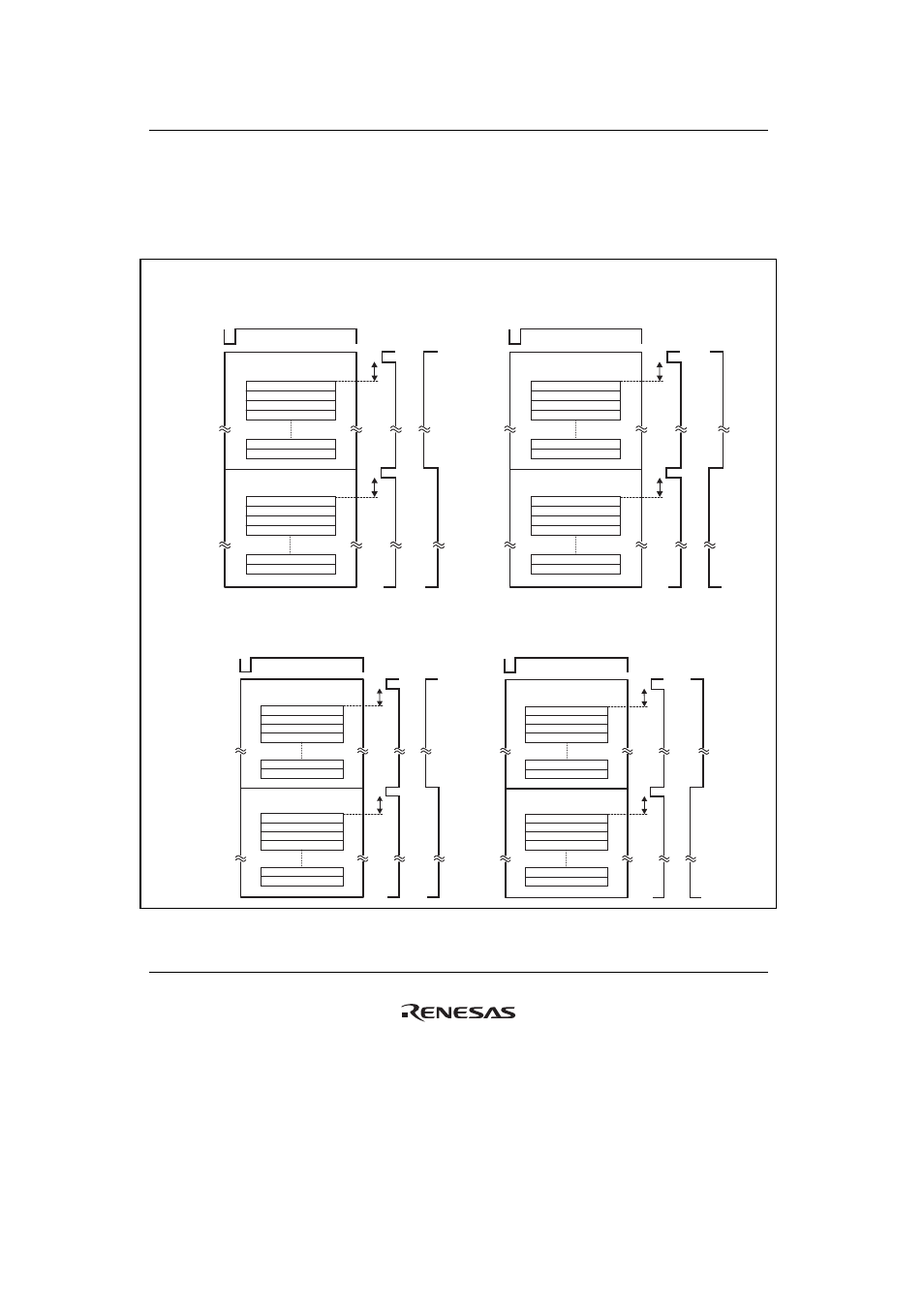
Figure 19.18 display in interlaced method – Renesas SH7781 User Manual
Page 994

19. Display Unit (DU)
Rev.1.00 Jan. 10, 2008 Page 964 of 1658
REJ09B0261-0100
• Display in interlaced method
At every scan period VC of the input video signal, even lines and odd lines are switched and
displayed in alternation, and a single screen (one frame) is combined and displayed (with the
afterimage of the preceding VC) with a period of 2VC. This is the normal TV input method.
1. Display in interlaced sync mode
When one frame is configured as shown below,
clear the ODEV bit to 0.
· The first field is an odd field (the ODDF pin is low)
· The second field is an even field (the ODDF pin is high)
When one frame is configured as shown below,
set the ODEV bit to 1.
· The first field is an even field (the ODDF pin is high)
· The second field is an odd field (the ODDF pin is low)
2. Display in interlaced sync & video mode
When one frame is configured as shown below,
clear the ODEV bit to 0.
· The first field is an odd field (the ODDF pin is low)
· The second field is an even field (the ODDF pin is high)
When one frame is configured as shown below,
set the ODEV bit to 1.
· The first field is an even field (the ODDF pin is high)
· The second field is an odd field (the ODDF pin is low)
0
1
2
3
238
239
HSYNC
VDS
Even field
VDS + HC/2
VSYNC
ODDF
0
1
2
3
238
239
Odd filed
0
2
4
6
476
478
HSYNC
VDS
Even field
VDS + HC/2
VSYNC
ODDF
1
3
5
7
477
479
Odd filed
0
1
2
3
238
239
HSYNC
VDS
Odd filed
VDS - HC/2
VSYNC
ODDF
0
1
2
3
238
239
Even field
1
3
5
7
477
479
HSYNC
VDS
Odd filed
VDS - HC/2
VSYNC
ODDF
0
2
4
6
476
478
Even field
Figure 19.18 Display in Interlaced Method
