4 csn wait control register (csnwcr) – Renesas SH7781 User Manual
Page 407
11. Local Bus State Controller (LBSC)
Rev.1.00 Jan. 10, 2008 Page 377 of 1658
REJ09B0261-0100
11.4.4
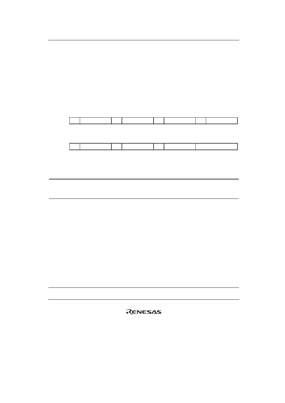
CSn Wait Control Register (CSnWCR)
CSnWCR (n = 0 to 6) are 32-bit readable/writable registers that specify the number of wait cycles
to be inserted for areas 0 to 6, the number of wait cycles to be inserted preceding the first data in
burst memory access, the address setup time, which is the time from the point at which the output
of address for access is started until assertion of the read/write strobe signal, and the number of
cycles to be inserted as the data hold time from negation of the write strobe signal.
CSnWCR is initialized to H'7777 770F by a power-on reset, but it is not initialized by a manual
reset.
16
17
18
19
20
21
22
23
24
25
26
27
28
29
31
30
1
1
1
0
1
1
1
0
1
1
1
0
1
1
0
1
RDH
⎯
RDS
⎯
ADH
⎯
ADS
⎯
R/W
R/W
R/W
R
R/W
R/W
R/W
R
R/W
R/W
R/W
R
R/W
R/W
R
R/W
BIt:
Initial value:
R/W:
⎯
⎯
0
1
2
3
4
5
6
7
8
9
10
11
12
13
15
14
1
1
1
1
0
0
0
0
1
1
1
0
1
1
0
1
IW[3:0]
BSH
WTH
WTS
⎯
R/W
R/W
R/W
R/W
R/W
R/W
R/W
R
R/W
R/W
R/W
R/W
R/W
R/W
R
R/W
BIt:
Initial value:
R/W:
Bit Bit
Name
Initial
Value R/W Description
31
⎯ 0
R
Reserved
This bit is always read as 0. The write value should
always be 0.
30 to 28 ADS
111
R/W
Address Setup Cycle
These bits specify the number of cycles to be inserted
as the address setup time with respect to
CSn
assertion. (Only valid when the SRAM interface, byte
control SRAM interface, or burst ROM interface is
selected.)
000: No cycle inserted
001: 1 cycle inserted
010: 2 cycles inserted
011: 3 cycles inserted
100: 4 cycles inserted
101: 5 cycles inserted
110: 6 cycles inserted
111: 7 cycles inserted