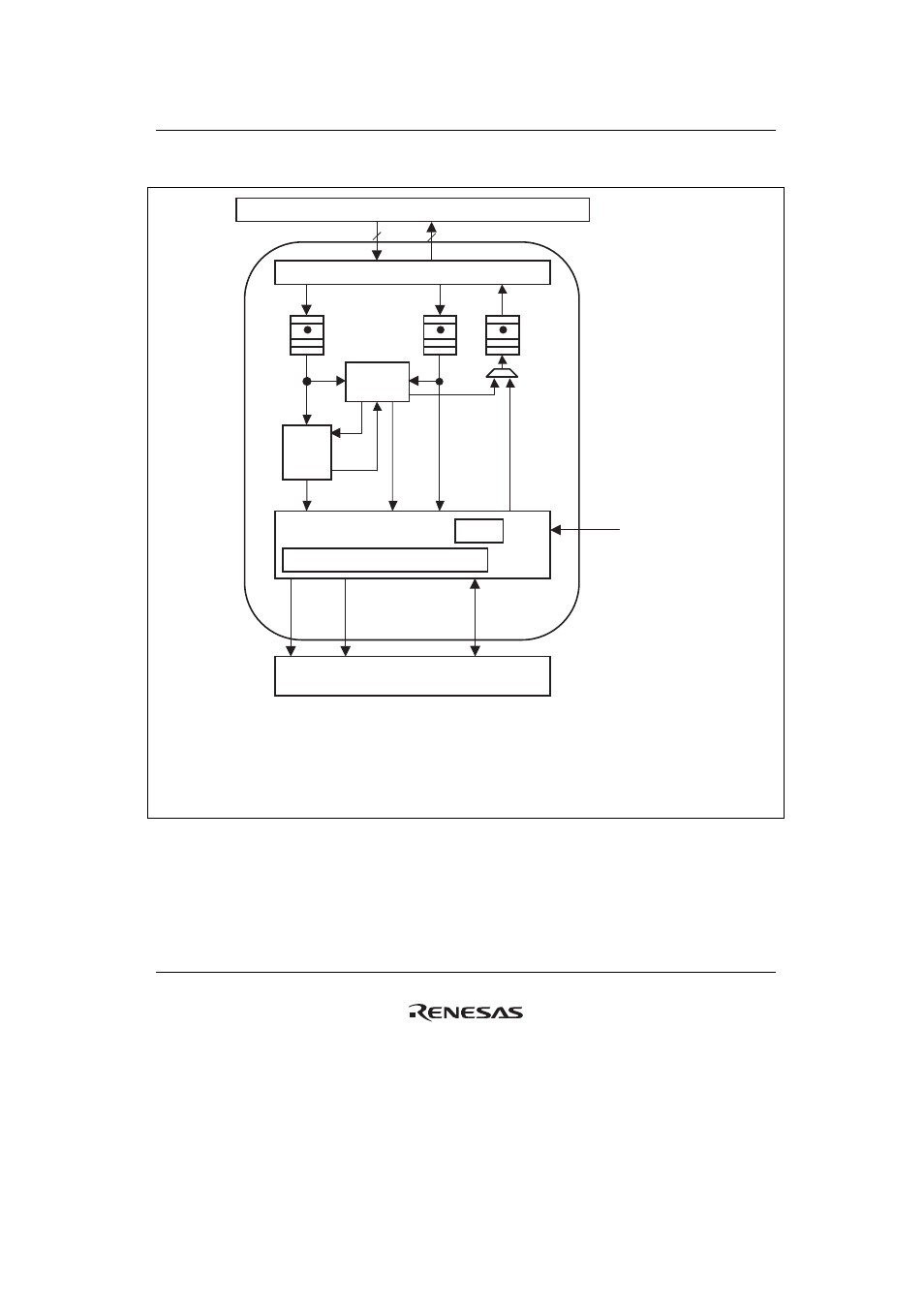
Figure 12.1 shows a block diagram of the dbsc2, Figure 12.1 block diagram of the dbsc2 – Renesas SH7781 User Manual
Page 489

12. DDR2-SDRAM Interface (DBSC2)
Rev.1.00 Jan. 10, 2008 Page 459 of 1658
REJ09B0261-0100
Figure 12.1 shows a block diagram of the DBSC2.
BUS IF
Request
queue
Control
unit
Registers
DDRPAD
DLL
IO cells
MDQS3 to MDQS0,
MDQS3 to MDQS0,
MDM3 to MDM0,
MDQ31 to MDQ0
MCKE, MA14 to MA0,
MBA2 to MBA0,
MCS,
MRAS, MCAS, MWE,
MODT
Write data
queue
Response
queue
SuperHyway Bus
DDR2-SDRAM
DBSC2
MCK0/
MCK0,
MCK1/
MCK1
MBKPRST, MVREF
Notes:
Request queue:
Write data queue:
Response queue:
Control unit:
Registers:
DDRPAD:
Stores the access request of the SuperHyway bus.
Stores the write data sent from the SuperHyway bus.
Stores the read data to be sent back to the SuperHyway bus.
Controls each block depending on the request sent from the request queue.
Store timing parameters and SDRAM configuration information.
Interfaces with the DDR2-SDRAM. This incorporates the DLL
to perform phase adjustment of the DQS.
Figure 12.1 Block Diagram of the DBSC2
- Single-Chip Microcomputer M34551T2-MCU (42 pages)
- M3T-FLX-80NRA (6 pages)
- 70 (162 pages)
- M16C/30P (102 pages)
- PROM Programming Adapter PCA7427G02 (20 pages)
- R0E572110CFK00 (40 pages)
- H8/325 Series (20 pages)
- Single-Chip Microcomputer H8/36079 (27 pages)
- Direct Dummy IC M3T-DIRECT100S (4 pages)
- M3A-2152 (95 pages)
- PCA7755D (6 pages)
- M16C/6N5 (106 pages)
- SH7085 (50 pages)
- QFP-144 (23 pages)
- H8/3834 Series (22 pages)
- RSKM16C62P (3 pages)
- H8/33937 (22 pages)
- Single-Chip Microcomputer H8SX/1622 (5 pages)
- E6000 (29 pages)
- PCA7400 (18 pages)
- PCA4738FF-64 (20 pages)
- SuperH HS7339KCU01HE (43 pages)
- M16C FAMILY (103 pages)
- PCA7412F-100 (20 pages)
- 4513 (210 pages)
- M34551E8FP (16 pages)
- Dummy IC M3T-SSOP36B-450 (4 pages)
- Emulation Pod M30100T3-RPD-E (52 pages)
- Converter Board for M30102 M30102T-PTC (4 pages)
- SH7145 (31 pages)
- HS1653ECN61H (36 pages)
- Converter Board R0E521276CFG00 (4 pages)
- PCA7302E1F-80 (18 pages)
- H8/3814 Series (21 pages)
- H8S/2646 Series (20 pages)
- SuperHTM Family SH7125 Series (40 pages)
- M30262T-PTC (4 pages)
- SH7670 (82 pages)
- H8/3864 Series (20 pages)
- Emulator System M3T-MR100 (306 pages)
- 38K0 (6 pages)
- PLQP0176KB-A (40 pages)
- Direct Dummy IC M3T-DIRECT80S (6 pages)
- PCA4738L-80A (26 pages)
- Converter Board R0E5212BACFG00 (6 pages)
