Renesas SH7781 User Manual
Page 1404

27. NAND Flash Memory Controller (FLCTL)
Rev.1.00 Jan. 10, 2008 Page 1374 of 1658
REJ09B0261-0100
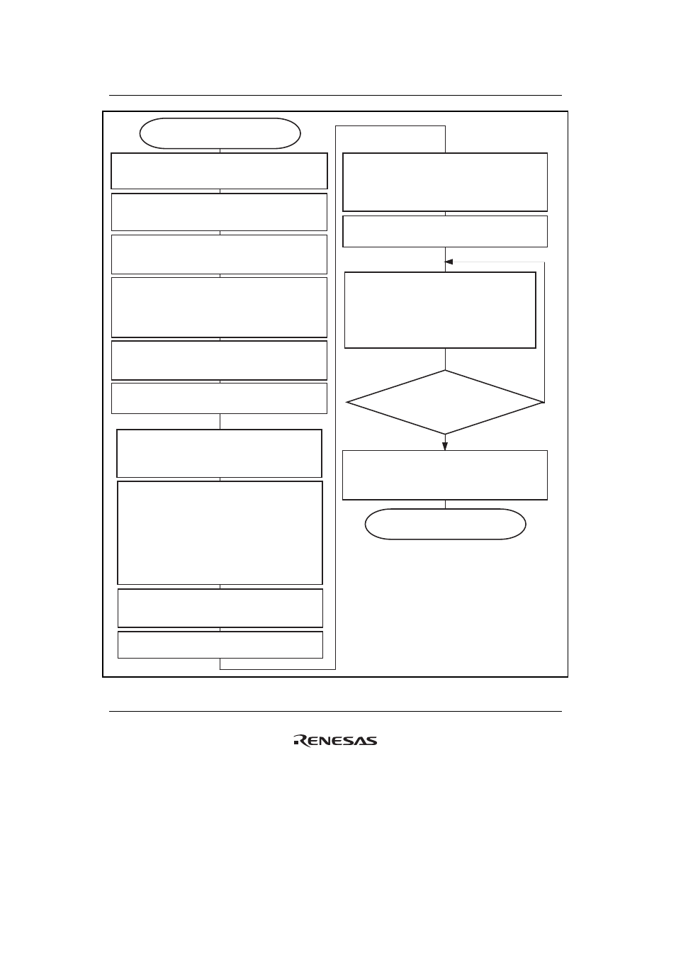
Start of sector access (flash write)
FLTRCR.TREND = B'1?
End of sector access (flash write)
DMA source address registers (SAR0 and SAR1)
SAR0[31:0]: Set start address of data to be written
SAR1[31:0]: Set start address of control code to be written
DMA destination address registers (DAR0 and DAR1)
DAR0[31:0]: Set FLDTFIFO address
DAR1[31:0]: Set FLECFIFO address
DMA transfer count registers (TCR0 and TCR1)
TCR0[31:0] = H'0000 0080 (512 bytes = 4
× 128)
TCR1[31:0] = H'0000 0004 (16 bytes = 4
× 4)
DMA channel control registers (CHCR0 and CHCR1)
SM[1:0] = B'01 (DMA transfer source address is
incremented)
RS[3:0] = B'1000 (DMA extended resource selector)
TS[2:0] = B'010 (longword transfer)
DE = B'1 (enable DMA transfer)
DMA extended resource selector (DMARS0)
DMARS0[15:0] = H'8783 (FLCTL data and control code
part transmission/reception)
DMA operation register (DMAOR)
DME = B'1 (enable DMA transfer for all channels)
Common control register (FLCMNCR)
ACM[1:0] = B'01 (sector access mode)
CE0 = B'1 (enable the chip)
TYPESEL = B'1 (select NAND-type flash memory)
Command control register (FLCMDCR)
SELRW = B'1 (flash write)
DOCMD1 = B'1 (execute first command stage)
DOCMD2 = B'1 (execute second command stage)
DOADR = B'1 (execute address stage)
ADRMD = B'1 (specify physical sector address)
ADRCNT[1:0] = B'10 (issue 3-byte address)
DOSR = B'1 (perform status read)
Specify number of sector transfers to SCTCNT[15:0]
(1 sector)
Command code register (FLCMCDR)
CMD[7:0] = H'80 (flash write command)
CMD[15:8] = H'10 (flash write execute command)
Address register (FLADR)
Specify physical sector address to ADR[17:0]
End of flash memory access
FLTRCR.TREND = 0 (clear processing end flag)
Read status
Check FLBSYCNT.STAT[7:0]
Perform flash memory writing
Issue first command
Issue address
Data stage (sector access)
Issue second command
Read status
Transfer control register (FLTRCR)
TRSTRT = B'1 (start flash memory access)
Interrupt DMA control register (FLINTDMACR)
DREQ1EN = B'1
(enable DMA transfer request from FLECFIFO)
DREQ0EN = B'1
(enable DMA transfer request from FLDTFIFO)
No
Yes
Figure 27.12 NAND Sector Access (Flash Write) Using DMAC
