2 frequency control register 1 (frqcr1) – Renesas SH7781 User Manual
Page 772
15. Clock Pulse Generator (CPG)
Rev.1.00 Jan. 10, 2008 Page 742 of 1658
REJ09B0261-0100
15.4.2
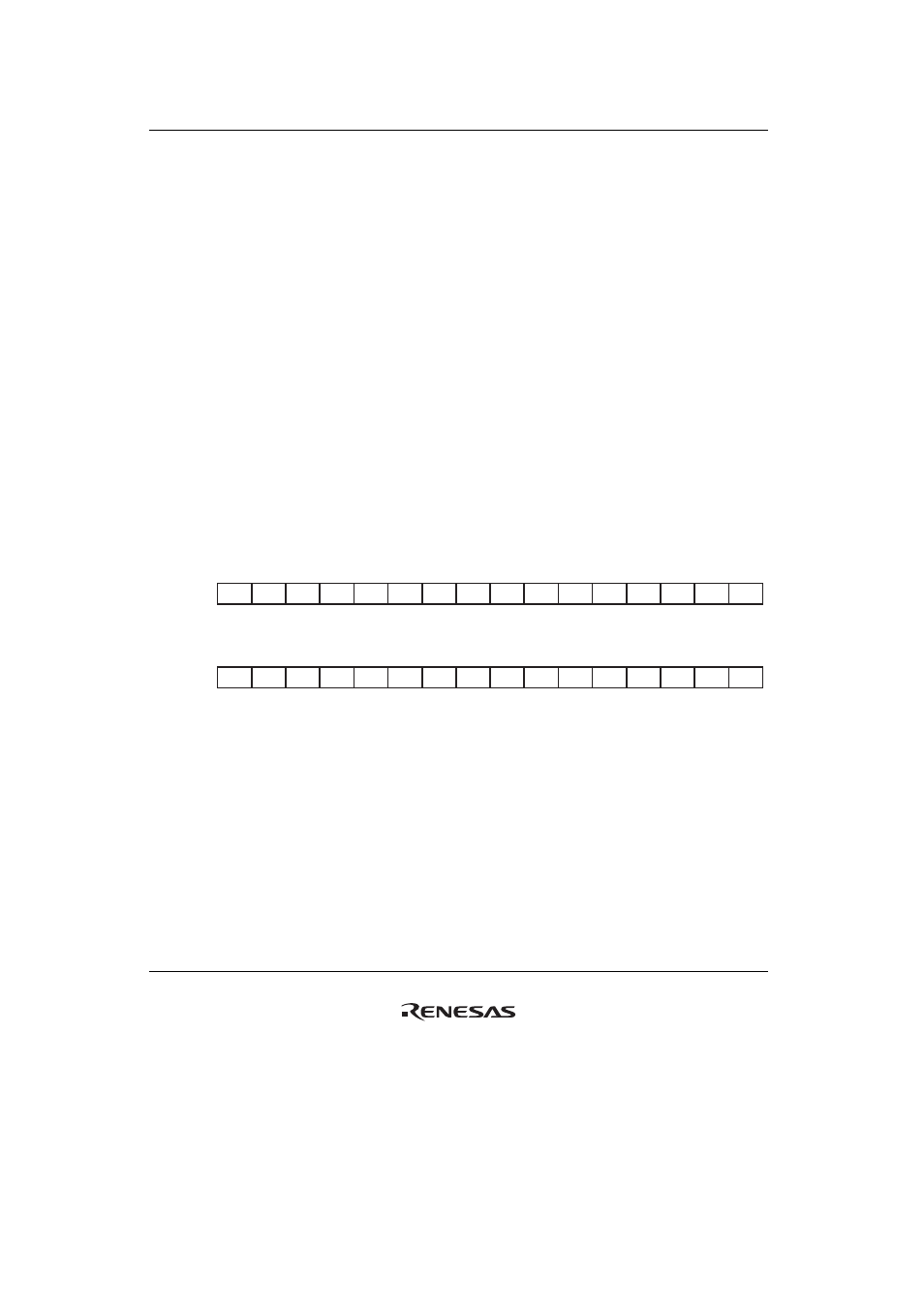
Frequency Control Register 1 (FRQCR1)
FRQCR1 is a 32-bit readable/writable register that can select the division ratio of divider 2 for the
CPU clock (lck), the SuperHyway clock (SHck), the peripheral clock (Pck), the DDR clock
(DDRck), the bus clock (Bck), the GDTA clock (GAck), the DU clock (DUck), and the RAM
clock (Uck). To check the division ratio of divider 2 for each clock, read FRQMR1. FRQCR1 can
only be accessed in longwords.
FRQCR1 only changes the division ratio of a clock to which a value other than H'0 has been
written. Therefore, set a value other than H'0 in the bit corresponding to the clock for which you
want to change the division ratio. Other bits should be set to H'0.
To change the division ratio of each clock to the value set in FRQCR1, you must set 1 in the
FRQE bit in FRQCR0 to execute the sequence that changes the frequency. After the sequence is
executed, this register is automatically cleared to H'0000 0000.
However, when changing the division ratio of the DDR clock (DDRck), switch SDRAM to the
self-refreshing state. For details on how to switch to or release the self-refreshing state, see section
12, DDR2-SDRAM Interface (DBSC2).
FRQCR1 is initialized by only a power-on reset via the
PRESET pin or a WDT overflow.
16
17
18
19
20
21
22
23
24
25
26
27
28
29
31
30
0
0
0
0
0
0
0
0
0
0
0
0
0
0
0
0
BFC0
BFC1
BFC2
BFC3
SFC0
SFC1
SFC2
SFC3
UFC0
UFC1
UFC2
UFC3
IFC0
IFC1
IFC3
IFC2
R/W
R/W
R/W
R/W
R/W
R/W
R/W
R/W
R/W
R/W
R/W
R/W
R/W
R/W
R/W
R/W
BIt:
Initial value:
R/W:
0
1
2
3
4
5
6
7
8
9
10
11
12
13
15
14
0
0
0
0
0
0
0
0
0
0
0
0
0
0
0
0
PFC0
PFC1
PFC2
PFC3
S3FC0
S3FC1
S3FC2
S3FC3
S2FC0
S2FC1
S2FC2
S2FC3
MFC0
MFC1
MFC3
MFC2
R/W
R/W
R/W
R/W
R/W
R/W
R/W
R/W
R/W
R/W
R/W
R/W
R/W
R/W
R/W
R/W
BIt:
Initial value:
R/W: