4 on-chip memory control register (ramcr) – Renesas SH7781 User Manual
Page 250
8. Caches
Rev.1.00 Jan. 10, 2008 Page 220 of 1658
REJ09B0261-0100
8.2.4
On-Chip Memory Control Register (RAMCR)
RAMCR controls the number of ways in the IC and OC and prediction of the IC way.
RAMCR modifications must only be made by a program in the non-cacheable P2 area. After
RAMCR has been updated, execute one of the following three methods before an access
(including an instruction fetch) to the cacheable area, the IL memory area, the OL memory area, or
the U memory area is performed.
1. Execute a branch using the RTE instruction. In this case, the branch destination may be the
non-cacheable area, the IL memory area, the OL memory area, or the U memory area.
2. Execute the ICBI instruction for any address (including non-cacheable area).
3. If the R2 bit in IRMCR is 0 (initial value) before updating RAMCR, the specific instruction
does not need to be executed. However, note that the CPU processing performance will be
lowered because the instruction fetch is performed again for the next instruction after RAMCR
has been updated.
Note that the method 3 may not be guaranteed in the future SuperH Series. Therefore, it is
recommended that the method 1 or 2 should be used for being compatible with the future SuperH
Series.
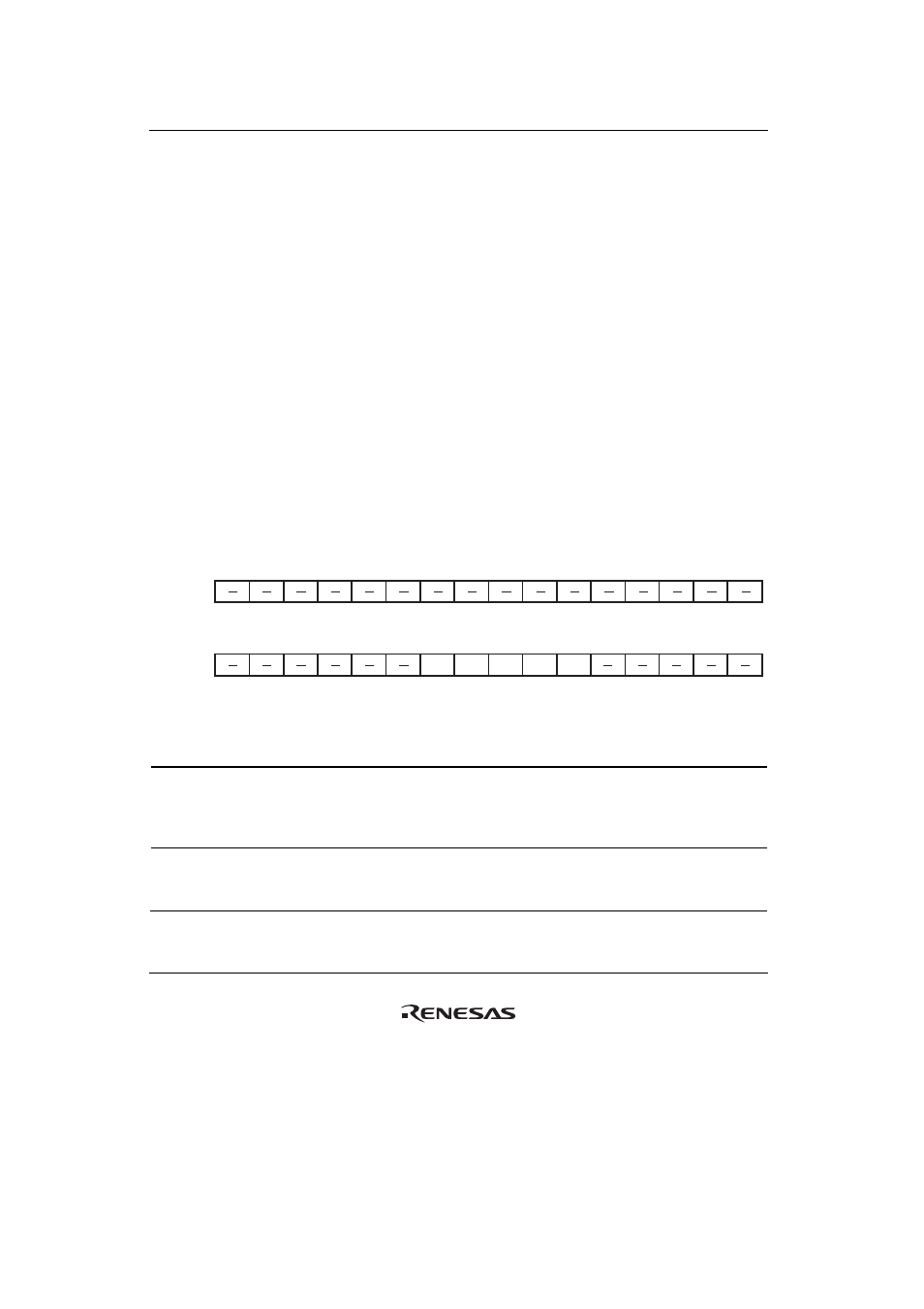
31
30
29
28
27
26
25
24
23
22
21
20
19
18
17
16
Bit:
Initial value:
R
R
R
R
R
R
R
R
R
R
RMD
RP
IC2W OC2W
R
R
R
R
R
R
0
0
0
0
0
0
0
0
0
0
0
0
0
0
0
0
0
0
0
0
0
0
0
0
0
0
0
0
0
0
0
0
R
R
R
R
R
R
R/W
R/W
R/W
R/W
R/W
R
R
R
R
R
R/W:
Bit:
Initial value:
R/W:
15
14
13
12
11
10
9
8
7
6
5
4
3
2
1
0
ICWPW
Bit Bit
Name
Initial
Value R/W
Description
31 to 10
⎯ All
0
R
Reserved
For details on reading from or writing to these bits, see
description in General Precautions on Handling of
Product.
9
RMD
0
R/W
On-Chip Memory Access Mode Bit
For details, see section 9.4, On-Chip Memory
Protective Functions.