1 common control register (flcmncr) – Renesas SH7781 User Manual
Page 1374
27. NAND Flash Memory Controller (FLCTL)
Rev.1.00 Jan. 10, 2008 Page 1344 of 1658
REJ09B0261-0100
27.3.1
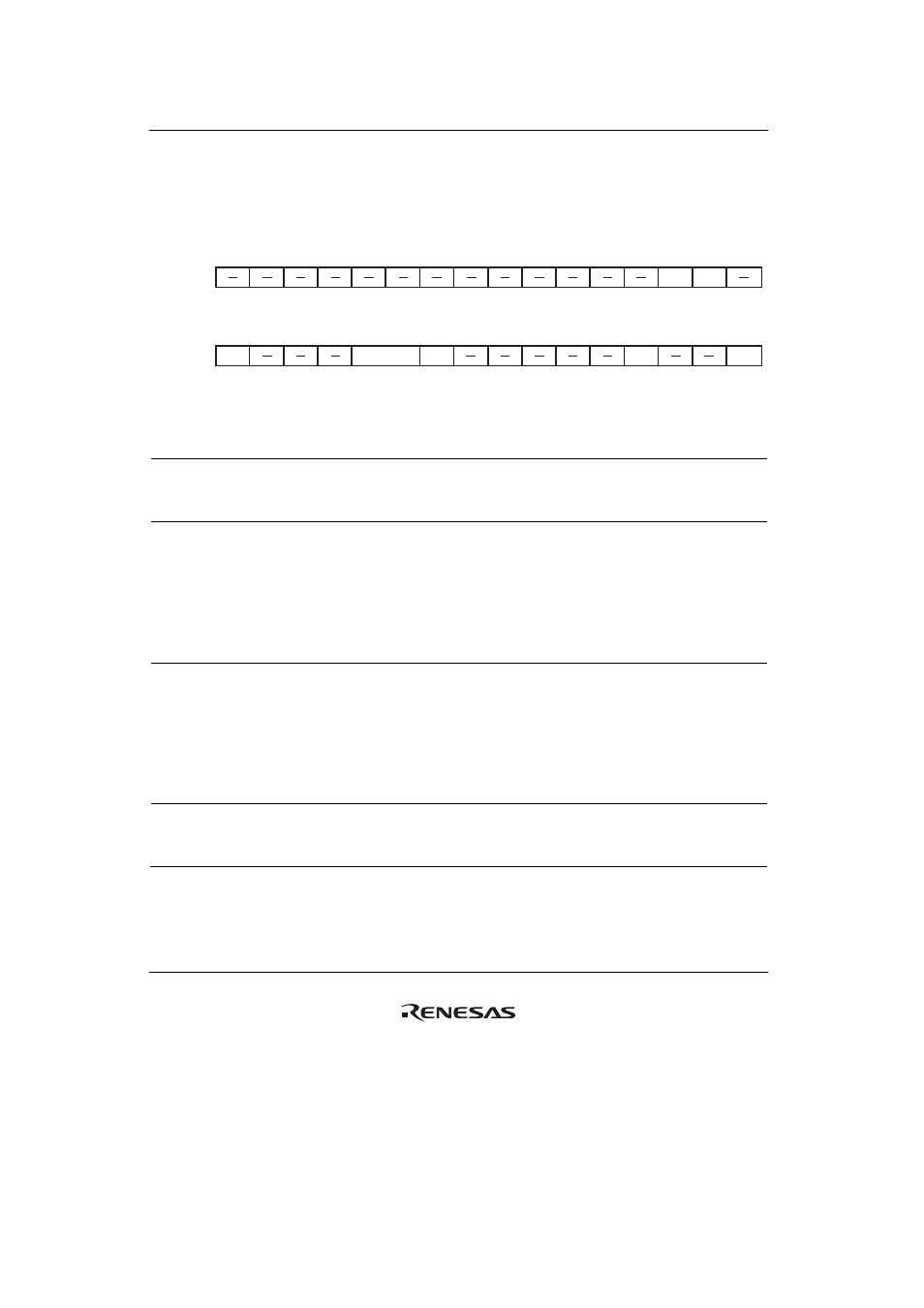
Common Control Register (FLCMNCR)
FLCMNCR is a 32-bit readable/writable register that specifies the type (NAND) of flash memory,
access mode, and
FCE pin output.
31
30
29
28
27
26
25
24
23
22
21
20
19
18
17
16
15
14
13
12
11
10
9
8
7
6
5
4
3
2
1
0
0
0
0
0
0
0
0
0
0
0
0
0
0
0
0
0
R
R
R
R
R
R
R
R
R
R
R
R
R
R/W
R/W
R
0
0
0
0
0
0
0
0
0
0
0
0
0
0
0
0
R/W
R
R
R
R/W
R/W
R/W
R
R
R
R
R
R/W
R
R
R/W
Bit:
Initial value:
R/W:
Bit:
Initial value:
R/W:
QTSEL
SNAND
FCK
SEL
ACM[1:0]
NAND
WF
CE0
TYPE
SEL
Bit Bit
Name
Initial
Value R/W Description
31 to 19 —
All 0
R
Reserved
These bits are always read as 0. The write value should
always be 0.
18
SNAND
0
R/W
Large Capacity NAND Flash Memory Select
This bit is used to specify the NAND flash memory that
a page consists of 2048
+ 64 bytes.
0: Selects the flash memory that a page consists of 512
+ 16 bytes
1: Selects the flash memory that a page consists of
2048
+ 64 bytes
17
QTSEL
0
R/W
Quarter Flash Clock Select
0: Uses the FCLK selected by the FCKSEL bit
1: Divides the operating clock of the FLCTL (a
peripheral clock) by four and uses it as the FCLK
when FCKSEL
= 0
Note: When FCKSEL
= 1, setting this bit to 1 is
prohibited.
16 — 0 R Reserved
This bit is always read as 0. The write value should
always be 0.