4 control registers, 4 control registers (1) status register (sr) – Renesas SH7781 User Manual
Page 63
2. Programming Model
Rev.1.00 Jan. 10, 2008 Page 33 of 1658
REJ09B0261-0100
2.2.4
Control Registers
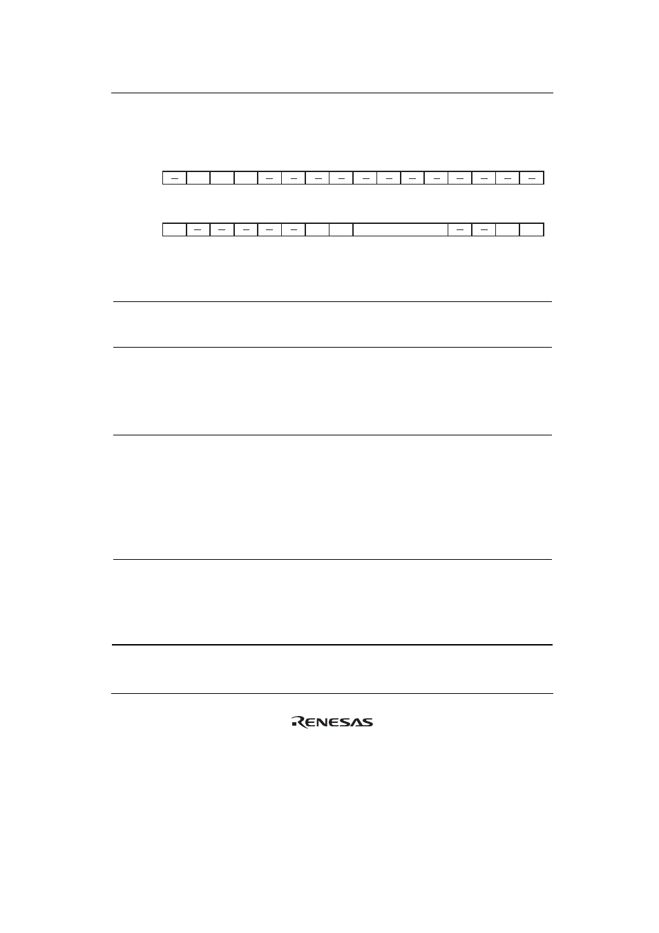
(1)
Status Register (SR)
31
30
29
28
27
26
25
24
23
22
21
20
19
18
17
16
BIt:
0
1
1
1
0
0
0
0
0
0
0
0
0
0
0
0
MD
RB
BL
FD
M
Q
IMASK
S
T
Initial value:
R
R/W
R/W
R/W
R
R
R
R
R
R
R
R
R
R
R
R
R/W:
15
14
13
12
11
10
9
8
7
6
5
4
3
2
1
0
BIt:
0
0
0
0
0
0
0
0
1
1
1
1
0
0
0
0
Initial value:
R/W
R
R
R
R
R
R/W
R/W
R/W
R/W
R/W
R/W
R
R
R/W
R/W
R/W:
Bit Bit
Name
Initial
Value R/W Description
31 —
0 R Reserved
For details on reading/writing this bit, see General
Precautions on Handling of Product.
30 MD
1 R/W
Processing
Mode
Selects the processing mode.
0: User mode (Some instructions cannot be executed
and some resources cannot be accessed.)
1: Privileged mode
This bit is set to 1 by an exception or interrupt.
29
RB
1
R/W
Privileged Mode General Register Bank Specification
Bit
0: R0_BANK0 to R7_BANK0 are accessed as general
registers R0 to R7 and R0_BANK1 to R7_BANK1 can
be accessed using LDC/STC instructions
1: R0_BANK1 to R7_BANK1 are accessed as general
registers R0 to R7 and R0_BANK0–R7_BANK0 can
be accessed using LDC/STC instructions
This bit is set to 1 by an exception or interrupt.
28
BL
1
R/W
Exception/Interrupt Block Bit
This bit is set to 1 by a reset, a general exception, or an
interrupt.
While this bit is set to 1, an interrupt request is masked.
In this case, this processor enters the reset state when
a general exception other than a user break occurs.