4 write-back buffer, 5 write-through buffer – Renesas SH7781 User Manual
Page 255

8. Caches
Rev.1.00 Jan. 10, 2008 Page 225 of 1658
REJ09B0261-0100
6. Cache miss (copy-back, with write-back)
The tag and data field of the cache line on the way which is selected to replace are saved in the
write-back buffer. Then a data write in accordance with the access size is performed for the
data field on the hit way which is indexed by virtual address bits [4:0]. Then, the data,
excluding the cache-missed data which is written already, is read into the cache line on the
way which is selected to replace from the physical address space corresponding to the virtual
address. Data reading is performed, using the wraparound method, in order from the quad-
word data (8 bytes) including the cache-missed data. While the remaining data on the cache
line is being read, the CPU can execute the next processing. When reading of one line of data
is completed, the tag corresponding to the physical address is recorded in the cache, 1 is
written to the V bit and the U bit on the way. Then the LRU bit is updated to indicate the way
is latest one. Then the data in the write-back buffer is then written back to external memory.
7. Cache miss (write-through)
A write of the specified access size is performed to the external memory corresponding to the
virtual address. In this case, a write to cache is not performed.
8.3.4
Write-Back Buffer
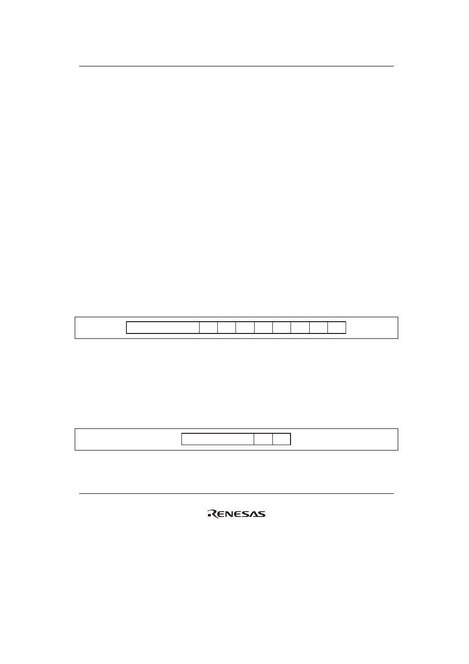
In order to give priority to data reads to the cache and improve performance, this LSI has a write-
back buffer which holds the relevant cache entry when it becomes necessary to purge a dirty cache
entry into external memory as the result of a cache miss. The write-back buffer contains one cache
line of data and the physical address of the purge destination.
LW7
Physical address bits [28:5]
LW6
LW5
LW4
LW3
LW2
LW1
LW0
Figure 8.3 Configuration of Write-Back Buffer
8.3.5
Write-Through Buffer
This LSI has a 64-bit buffer for holding write data when writing data in write-through mode or
writing to a non-cacheable area. This allows the CPU to proceed to the next operation as soon as
the write to the write-through buffer is completed, without waiting for completion of the write to
external memory.
Physical address bits[28:0]
LW1
LW0
Figure 8.4 Configuration of Write-Through Buffer
