1 address spaces, Figure 7.2 virtual address space (at in mmucr = 0) – Renesas SH7781 User Manual
Page 176
7. Memory Management Unit (MMU)
Rev.1.00 Jan. 10, 2008 Page 146 of 1658
REJ09B0261-0100
7.1.1
Address Spaces
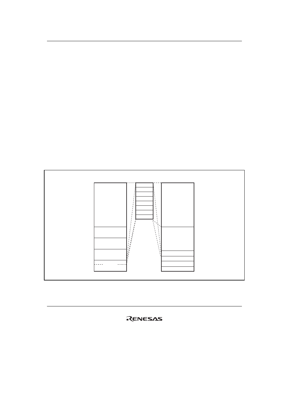
(1)
Virtual Address Space
This LSI supports a 32-bit virtual address space, and can access a 4-Gbyte address space. The
virtual address space is divided into a number of areas, as shown in figures 7.2 and 7.3. In
privileged mode, the 4-Gbyte space from the P0 area to the P4 area can be accessed. In user mode,
a 2-Gbyte space in the U0 area can be accessed. When the SQMD bit in the MMU control register
(MMUCR) is 0, a 64-Mbyte space in the store queue area can be accessed. When the RMD bit in
the on-chip memory control register (RAMCR) is 1, a 16-Mbyte space in on-chip memory area
can be accessed. Accessing areas other than the U0 area, store queue area, and on-chip memory
area in user mode will cause an address error.
When the AT bit in MMUCR is set to 1 and the MMU is enabled, the P0, P3, and U0 areas can be
mapped onto any physical address space in 1-, 4-, 64-Kbyte, or 1-Mbyte page units in TLB
compatible mode and in 1-, 4-, 8-, 64-, 256-Kbyte, 1-, 4-, or 64-Mbyte page units in TLB extended
mode. By using an 8-bit address space identifier, the P0, P3, and U0 areas can be increased to a
maximum of 256. Mapping from the virtual address space to the 29-bit physical address space is
carried out using the TLB.
H'0000 0000
H'8000 0000
H'E000 0000
H'E400 0000
H'E500 0000
H'E600 0000
H'FFFF FFFF
H'0000 0000
H'8000 0000
H'FFFF FFFF
H'A000 0000
H'C000 0000
H'E000 0000
Area 0
Area 1
Area 2
Area 3
Area 4
Area 5
Area 6
Area 7
Physical
address space
Address error
Address error
Address error
On-chip memory area
Store queue area
User mode
Privileged mode
P1 area
Cacheable
P0 area
Cacheable
P2 area
Non-cacheable
P3 area
Cacheable
P4 area
Non-cacheable
U0 area
Cacheable
Figure 7.2 Virtual Address Space (AT in MMUCR = 0)