5 example of register setting – Renesas SH7781 User Manual
Page 1403

27. NAND Flash Memory Controller (FLCTL)
Rev.1.00 Jan. 10, 2008 Page 1373 of 1658
REJ09B0261-0100
27.5
Example of Register Setting
The examples of setting and starting registers in each access mode are shown below.
No
Yes
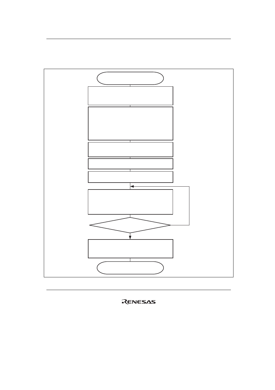
FLTRCR.TREND = B'1?
End of command access (block erase)
Start of command access (block erase)
Common control register (FLCMNCR)
ACM[1:0] = B'00 (command access mode)
CE0 = B'1 (enable the chip)
TYPESEL = B'1 (select NAND-type flash memory)
Command control register (FLCMDCR)
DOCMD1 = B'1 (execute first command stage)
DOCMD2 = B'1 (execute second command stage)
DOADR = B'1 (execute address stage)
ADRMD = B'1 (address register value is output as
memory address)
ADRCNT[1:0] = B'01 (issue 2-byte address)
DOSR = B'1 (perform status read)
Command code register (FLCMCDR)
CMD[7:0] = H'60 (block erase command)
CMD[15:8] = H'D0 (block erase execute command)
Address register (FLADR)
Set erase addresses to ADR[7:0] and ADR[15:8]
Transfer control register (FLTRCR)
TRSTRT = B'1 (start flash memory access)
Perform block erase of flash memory
Issue first command
Issue address
Issue second command
Read status
Set TRSTRT = B'1 (start flash memory access)
End of flash memory access
FLTRCR.TREND = B'0 (clear processing end flag)
Read status
Check FLBSYCNT.STAT[7:0]
Figure 27.11 NAND Command Access (Block Erase)
