Renesas SH7781 User Manual
Page 278
9. On-Chip Memory
Rev.1.00 Jan. 10, 2008 Page 248 of 1658
REJ09B0261-0100
Bit Bit
Name
Initial
Value R/W
Description
6
OC2W
0
R/W
OC Two-Way Mode
For further details, refer to section 8.3.6, OC Two-Way
Mode.
5
ICWPD
0
R/W
IC Way Prediction Disable
For further details, refer to section 8.4.4, Instruction
Cache Way Prediction Operation.
4 to 0
—
All 0
R
Reserved
For read/write in these bits, refer to General
Precautions on Handling of Product.
9.2.2
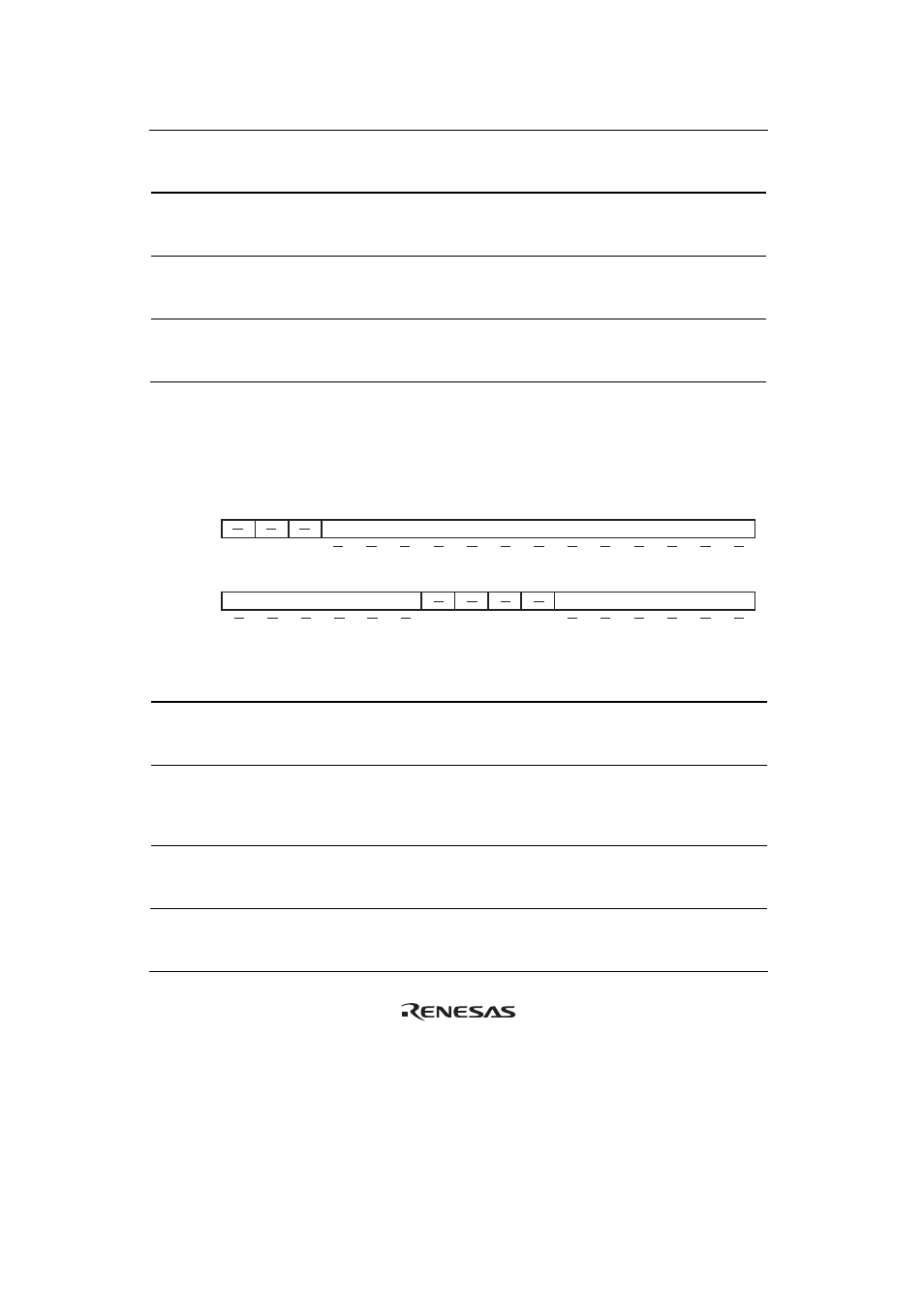
OL memory Transfer Source Address Register 0 (LSA0)
When MMUCR.AT = 0 or RAMCR.RP = 0, the LSA0 specifies the transfer source physical
address for block transfer to page 0A or 0B of the OL memory.
31
30
29
28
27
26
25
24
23
22
21
20
19
18
17
16
Bit :
0
0
0
Initial value :
R
R
R
R/W
R/W
R/W
R/W
R/W
R/W
R/W
L0DADR
L0DADR
L0DSZ
R/W
R/W
R/W
R/W
R/W
R/W
R/W:
15
14
13
12
11
10
9
8
7
6
5
4
3
2
1
0
Bit :
0
0
0
0
Initial value :
R/W
R/W
R/W
R/W
R/W
R/W
R
R
R
R
R/W
R/W
R/W
R/W
R/W
R/W
R/W:
Bit Bit
Name
Initial
Value R/W
Description
31 to 29 —
All 0
R
Reserved
For read/write in these bits, refer General Precautions
on Handling of Product.
28 to 10 L0SADR
Undefined R/W
OL memory Page 0 Block Transfer Source Address
When MMUCR.AT = 0 or RAMCR.RP = 0, these bits
specify the transfer source physical address for block
transfer to page 0A or 0B in the OL memory.
9 to 6
—
All 0
R
Reserved
For read/write in these bits, refer to General
Precautions on Handling of Product.