7 notes on designing board – Renesas SH7781 User Manual
Page 786

15. Clock Pulse Generator (CPG)
Rev.1.00 Jan. 10, 2008 Page 756 of 1658
REJ09B0261-0100
15.7
Notes on Designing Board
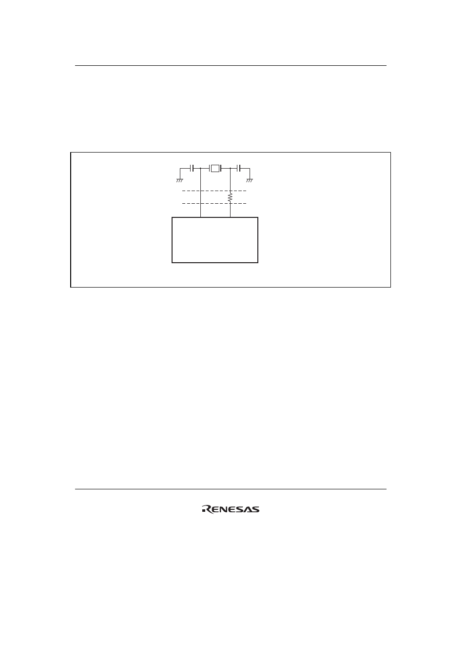
1. Note on Using a Crystal Resonator
Place the crystal resonator and capacitors close to the EXTAL and XTAL pins as much as
possible. No other signal lines should cross the signal line of these pins. Induction may prevent
correct oscillation.
EXTAL
XTAL
SH7785
CL1
CL2
R
Crossing of signal lines
is prohibited
Recommended values
CL1 = CL2 = 0 to 33 pF
R = 0
Ω
Note: The values of CL1, CL2, and the dumping resistance should be determined through
evaluation and consultation with the manufacturer of the crystal resonator to be used.
Figure 15.4 Note on Using a Crystal Resonator
2. Note on Inputting the External Clock from the EXTAL Pin
Do not connect anything to the XTAL pin.
3. Note on Using a PLL Oscillator Circuit
Place VDDQ-PLL1, VDDQ-PLL2, VSSQ-PLL1, and VSSQ-PLL2 away from other VDDs
and VSSs on the power supply of the board. Insert resistors RCB, and bypass capacitors, CPB
and CB, as noise filters near the pins.
