Figure 19.1 block diagram of the display unit (du) – Renesas SH7781 User Manual
Page 849
19. Display Unit (DU)
Rev.1.00 Jan. 10, 2008 Page 819 of 1658
REJ09B0261-0100
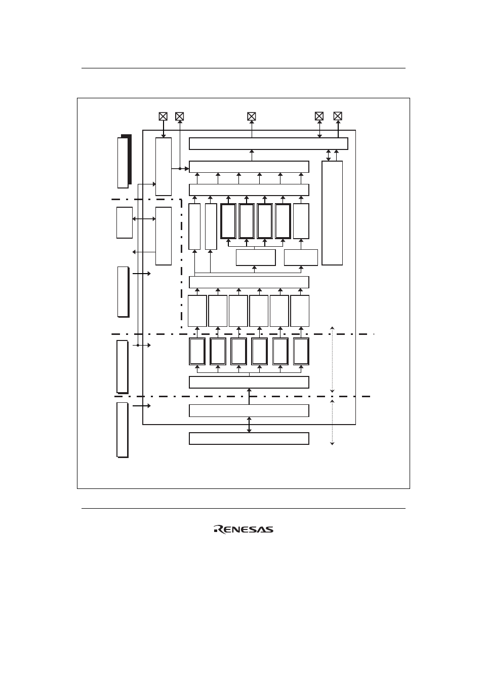
Figure 19.1 shows a block diagram of the display unit (DU).
Pin control (output timing adjustment)
Display data format selection
Priority contention
determination
16 bit/pixel
(no conversion)
YC to RGB
conversion
Display timin
g
g
eneration
Color palette
contention
determination
YC conversion
contention
determination
Plane rearrangement by priority
1 pixel division
Transparent
color
determination
1 pixel division
Transparent
color
determination
1 pixel division
Transparent
color
determination
1 pixel division
Transparent
color
determination
1 pixel division
Transparent
color
determination
1 pixel division
Transparent
color
determination
Endian conversion
SHwy packet router
Dot clock
g
eneration
(frequency division circuit)
Superposition (
α blending, EOR operation)
Peripheral bus interface
Peripheral
bus
SHwy interface
irq
Dot clock area
Peripheral clock area
128-bit bus
SHck
64-bit bus
DU clock area
SHwy clock area
DUck
Pck
Color palette 2
(26b x 256w)
Color palette 3
(26b x 256w)
Color palette 4
(26b x 256w)
Color palette 1
(26b x 256w)
DCLKIN DCLKOUT
DR5 to DR0
DG5 to DG0
DB5 to DB0
HSYNC
VSYNC
ODDF
DISP
CDE
Buffer-1
(128B x 3)
Buffer-2
(128B x 3)
Buffer-3
(128B x 3)
Buffer-4
(128B x 3)
Buffer-5
(128B x 3)
Buffer-6
(128B x 3)
Legend:
B: byte
b: bit
w: word
Figure 19.1 Block Diagram of the Display Unit (DU)