2 input/output pins – Renesas SH7781 User Manual
Page 1069
21. Serial Communication Interface with FIFO (SCIF)
Rev.1.00 Jan. 10, 2008 Page 1039 of 1658
REJ09B0261-0100
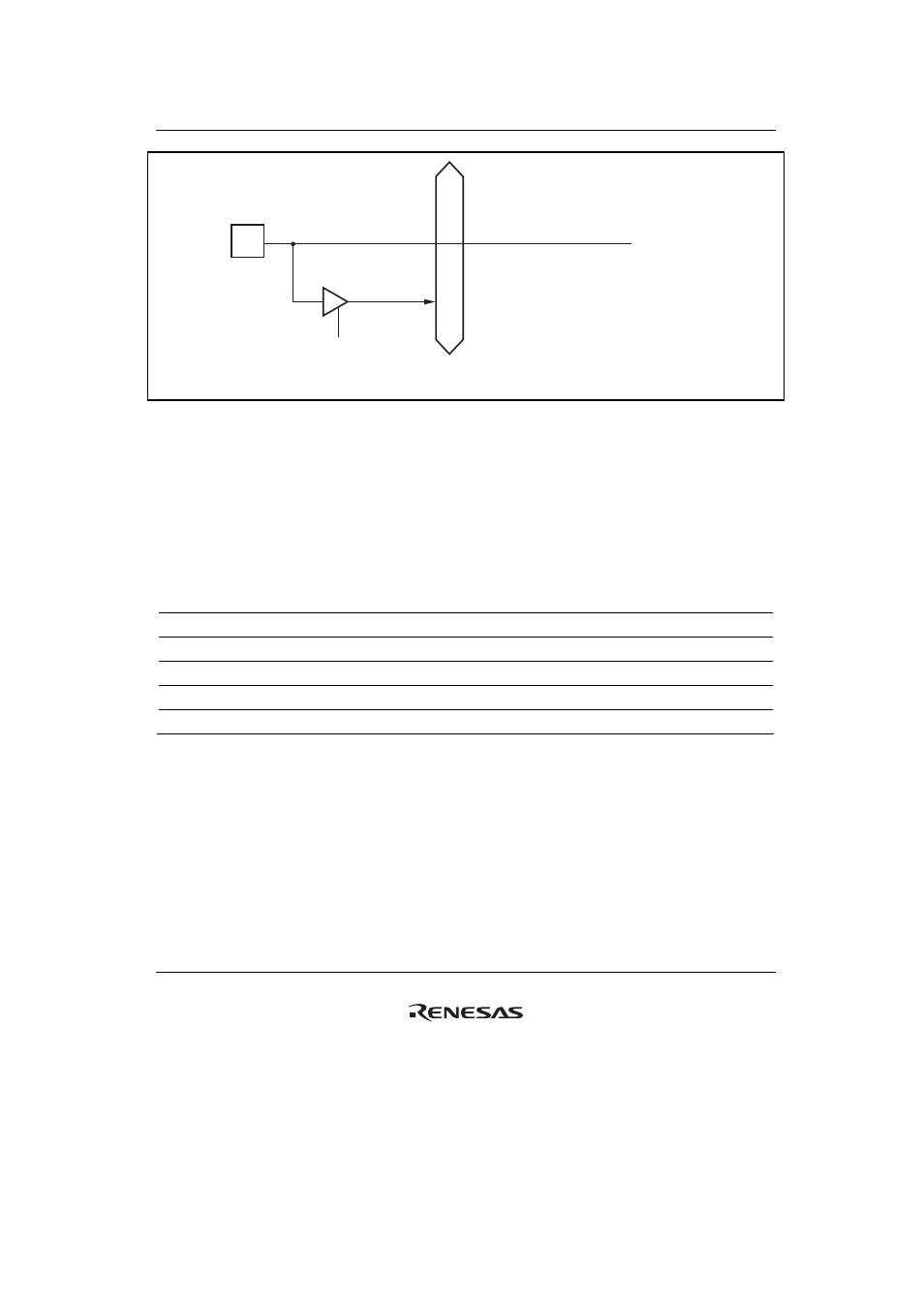
SPTRR
Legend:
SPTRR: Read from SCSPTR
SCIFn_RXD
Peripheral bus
Serial receive data
Figure 21.6 SCIFn_RXD Pin (n
= 0 to 5)
21.2
Input/Output Pins
Table 21.1 shows the SCIF pin configuration. Since the pin functions are the same in each
channel, the channel number is omitted in the description below. The modem control pins are
available only in channel 0.
Table 21.1 Pin Configuration
Pin Name
Abbreviation
I/O
Function
Serial clock pin
SCIF0_SCK to SCIF5_SCK
I/O
Clock input/output
Receive data pin
SCIF0_RXD to SCIF5_RXD
Input
Receive data input
Transmit data pin
SCIF0_TXD to SCIF5_TXD Output
Transmit
data
output
Modem control pin
SCIF0_CTS
I/O
Transmission enabled
Modem control pin
SCIF0_RTS
I/O
Transmission request
Note: These pins function as serial pins by performing SCIF operation settings with the C/
A bit in
SCSMR, the TE, RE, CKE1, and CKE0 bits in SCSCR, and the MCE bit in SCFCR. Break
state transmission and detection can be set by SCSPTR of the SCIF.