11 data fifo register (fldtfifo) – Renesas SH7781 User Manual
Page 1391
27. NAND Flash Memory Controller (FLCTL)
Rev.1.00 Jan. 10, 2008 Page 1361 of 1658
REJ09B0261-0100
27.3.11
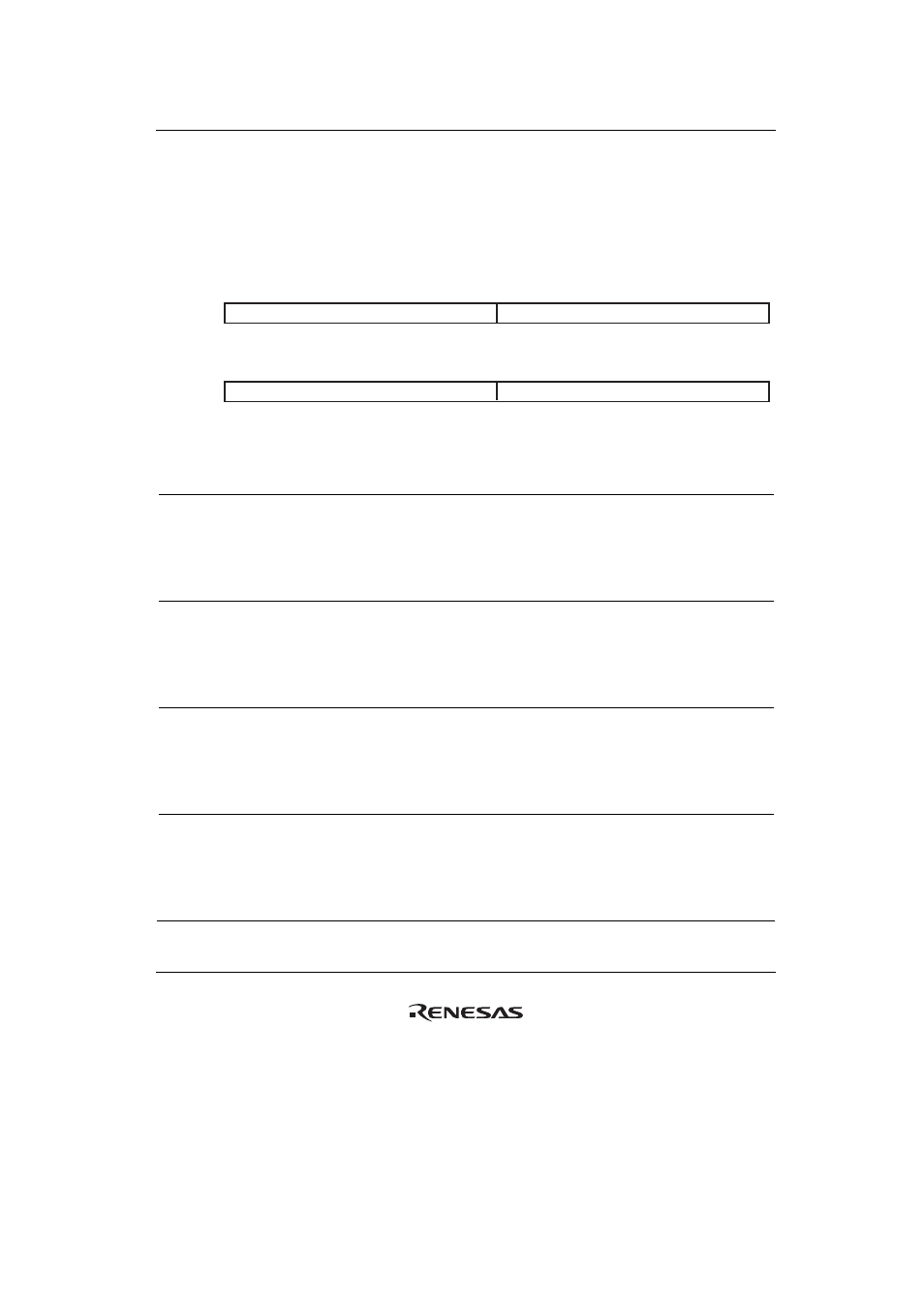
Data FIFO Register (FLDTFIFO)
FLDTFIFO is used to read from or write to the data FIFO area.
The read and write directions specified by the SELRW bit in FLCMDCR must match the read or
write access directions specified in this register.
31
30
29
28
27
26
25
24
23
22
21
20
19
18
17
16
15
14
13
12
11
10
9
8
7
6
5
4
3
2
1
0
R/W
R/W
R/W
R/W
R/W
R/W
R/W
R/W
R/W
R/W
R/W
R/W
R/W
R/W
R/W
R/W
R/W
R/W
R/W
R/W
R/W
R/W
R/W
R/W
R/W
R/W
R/W
R/W
R/W
R/W
R/W
R/W
Bit:
Initial value:
R/W:
Bit:
Initial value:
R/W:
DTFO[31:24]
DTFO[23:16]
DTFO[15:8]
DTFO[7:0]
—
—
—
—
—
—
—
—
—
—
—
—
—
—
—
—
—
—
—
—
—
—
—
—
—
—
—
—
—
—
—
—
Bit Bit
Name
Initial
Value R/W Description
31 to 24 DTFO[31:24]
⎯ R/W
First
Data
Specify the first data to be input or output via the FD7 to
FD0 pins.
In writing: Specify write data
In reading: Store read data
23 to 16 DTFO[23:16]
⎯ R/W
Second
Data
Specify the second data to be input or output via the FD7
to FD0 pins.
In writing: Specify write data
In reading: Store read data
15 to 8
DTFO[15:8]
⎯ R/W
Third
Data
Specify the third data to be input or output via the FD7 to
FD0 pins.
In writing: Specify write data
In reading: Store read data
7 to 0
DTFO[7:0]
⎯ R/W
Fourth
Data
Specify the fourth data to be input or output via the FD7
to FD0 pins.
In writing: Specify write data
In reading: Store read data