Renesas SH7781 User Manual
Page 1399

27. NAND Flash Memory Controller (FLCTL)
Rev.1.00 Jan. 10, 2008 Page 1369 of 1658
REJ09B0261-0100
(1)
Physical Sector
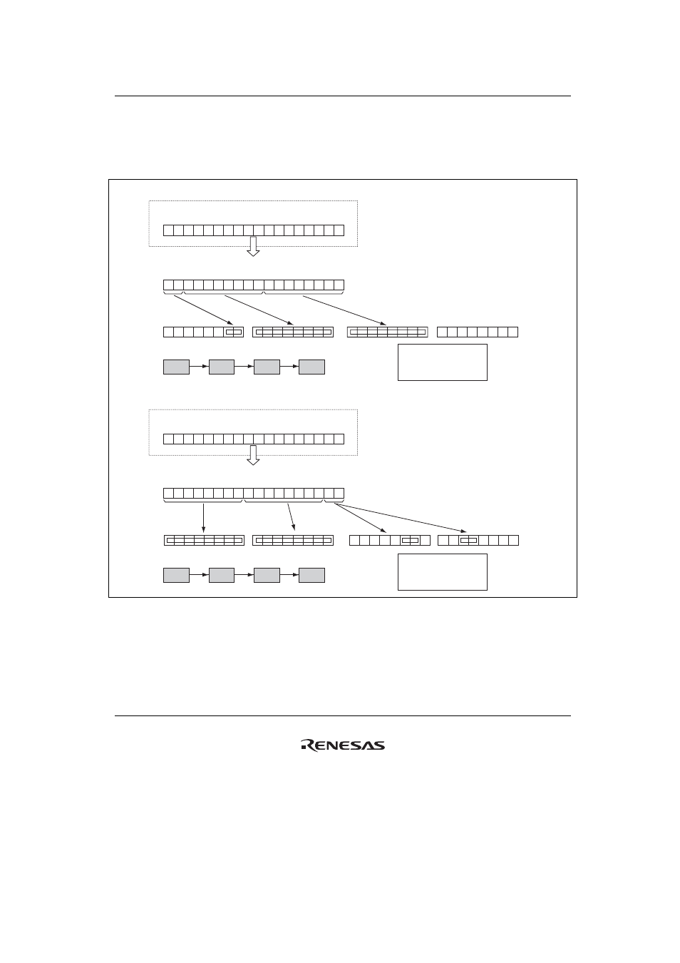
Figure 27.9 shows the relationship between the physical sector address and flash memory address
of NAND-type flash memory.
Bit 17
Bit 0
Row3
Row3
Row2
Row2
Row1
Col: Column address
Row: Row address
(Page address)
Bit 17
Bit 0
Bit 17
Bit 0
0 0 0 0 0 0
Col
0 0 0 0 0 0 0 0
Row1
Row2
Row1
Row2
Row1
Col
Bit 17
Bit 0
0 0
0 0
0 0
0 0 0 0 0
0
Col1
Col2
Col: Column address
Row: Row address
(Page address)
Col
Row1
Row2
Row3
Col1
Col2
Row1
Row2
Physical sector address
• For NAND-type flash memory (512 + 16 bytes)
Physical sector address bits (FLADR[17:0])
Order of address output to NAND-type flash memory I/O
• For NAND-type flash memory (2048 + 64 bytes)
Physical sector address
Physical sector address bits (FLADR[17:0])
Order of address output to NAND-type flash memory I/O
Note: Since the address at each boundary
(512 + 16 bytes) of a column address is
generated by FLADR[1:0], when using
NAND-type flash memory (2048 + 64 bytes),
set FLADR[1:0] as follows:
00: Address at byte 0
01: Address at (512 + 16)th byte
10: Address at (1024 + 32)th byte
11: Address at (1536 + 48)th byte
Figure 27.9 Example of Sector Number and NAND-Type Flash Memory Address
Expansion
