Renesas SH7781 User Manual
Page 447
11. Local Bus State Controller (LBSC)
Rev.1.00 Jan. 10, 2008 Page 417 of 1658
REJ09B0261-0100
complement mode. To access the Device Control Register and Alternate Status Register, use a
CPU byte access (do not use a DMA transfer), and to access the Data Register, use the CPU word
access (do not use a DMA transfer). To access the Data Port use a DMA transfer. When a CPU
byte access is executed,
CE1x is negated and CE2x is asserted (x = A, B). When a CPU word
access is executed,
CE1x is asserted and CE2x is negated. When a DMA access is executed, CE1x
and CE2x are negated. The setting example of the DMAC (by DMA channel control register
CHCR) is external request, burst mode, level detection, overrun 0,
DACK output to the
correspondent PCMCIA connected area. Set the DACKBST bit in BCR of the corresponding
DMA transfer channel to 1, so that the corresponding
DACK signal is asserted from the beginning
to the end of the DMA transfer cycle. Even if the corresponding
DREQ signal is negated during
the transfer, the
DACK signal is not negated. When DMA transfer that outputs DACK is made to
access an area where ATA complement mode is set, neither
CE1x nor CE2x is asserted.
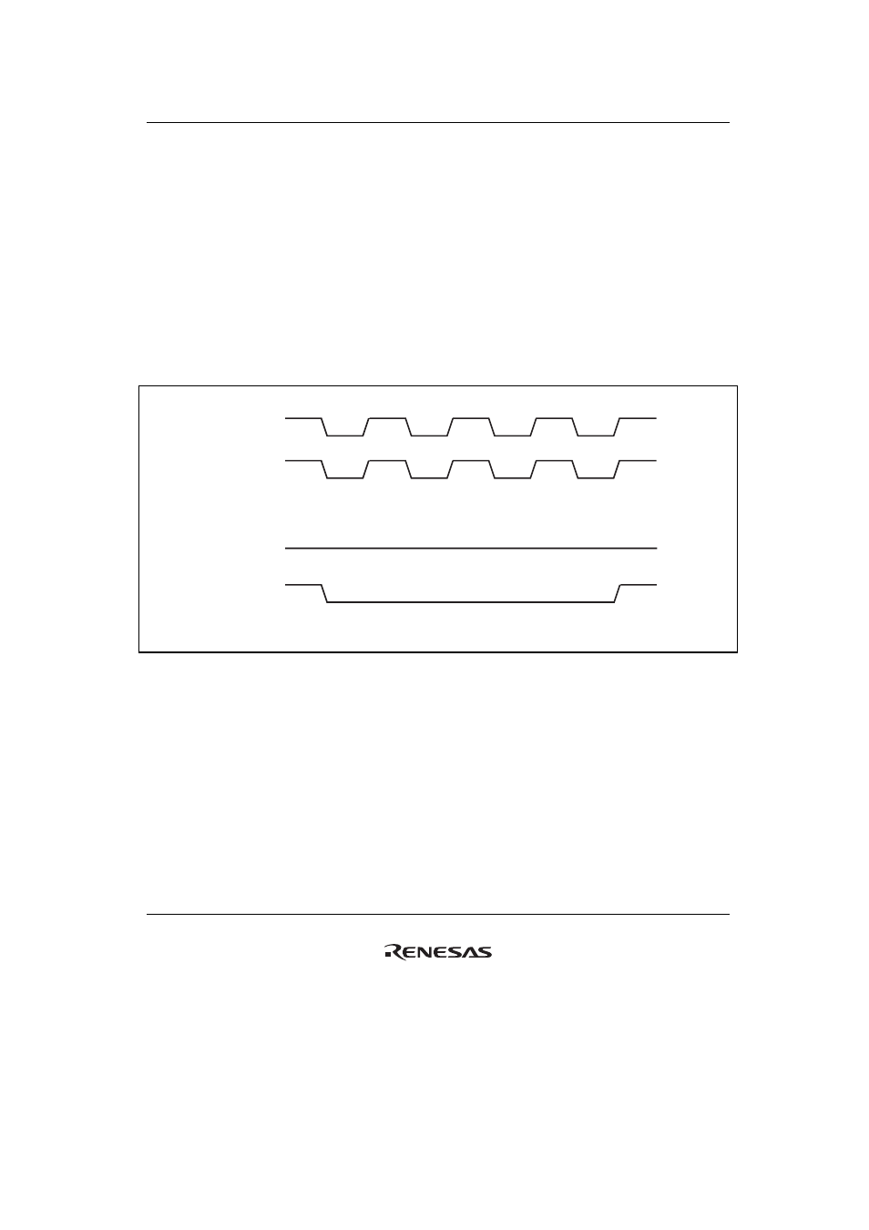
IO card interface, DACKBST = 0
ATA complement mode, DACKBST = 1
In this example, the number of DMA transfers = 4, transfer size = word, and DACKn is active-low.
CExx
DACKn
CExx
DACKn
Figure 11.15
CExx and DACKn Output during DMA Transfer in Access to Space where
ATA Complement Mode Is Set