13 cl control register (clcr) – Renesas SH7781 User Manual
Page 1021
20. Graphics Data Translation Accelerator (GDTA)
Rev.1.00 Jan. 10, 2008 Page 991 of 1658
REJ09B0261-0100
2. Setting Method When Setting Values in Succession
When setting values in this register in succession, the CL module is able to receive the
next command while the CL_CFF bit in CLSR is 0. To perform processing by changing
the command alone, just set the new command in this register.
3. The input Y/U/V pointers and output pointers must be set to point to addresses on 32-
byte boundaries. If not, the lower address is regarded as 0.
4. Two commands can be received. If the next command is written when the command
FIFO is full, the commands stored in the command FIFO are retained and the next
command is ignored.
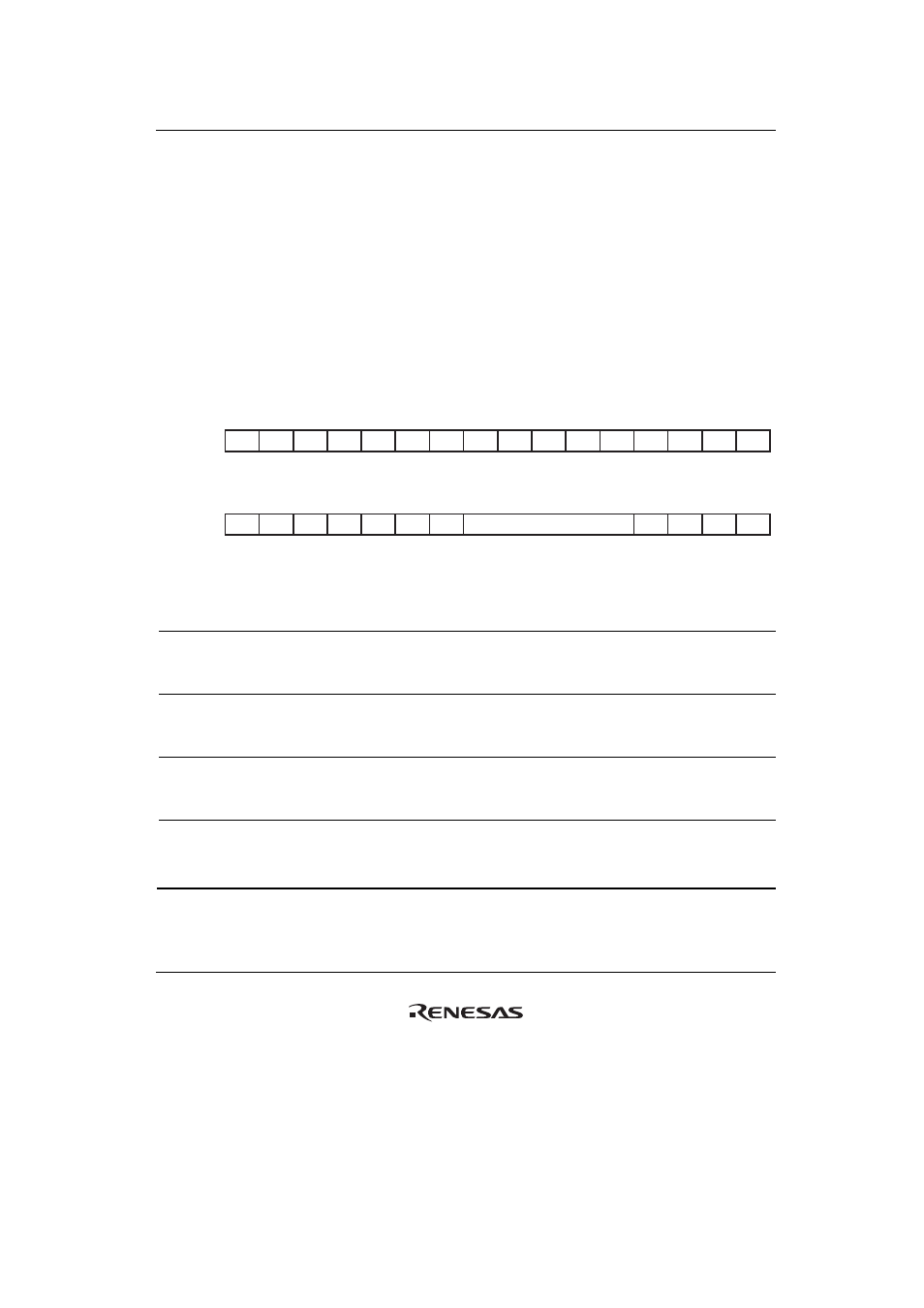
20.3.13
CL Control Register (CLCR)
CLCR is in the CL register block and specifies the CL operating mode.
16
17
18
19
20
21
22
23
24
25
26
27
28
29
31
30
0
0
0
0
0
0
0
0
0
0
0
0
0
0
0
0
⎯
⎯
⎯
⎯
⎯
⎯
⎯
⎯
⎯
⎯
⎯
⎯
⎯
⎯
⎯
⎯
⎯
⎯
⎯
⎯
⎯
⎯
⎯
⎯
⎯
⎯
⎯
⎯
⎯
⎯
⎯
⎯
BIt:
Initial value:
R/W:
0
1
2
3
4
5
6
7
8
9
10
11
12
13
15
14
0
0
0
0
0
0
0
0
0
0
0
0
0
0
0
0
CL_MD
CL_OA
CL_OD
⎯
CL_DA
⎯
⎯
⎯
⎯
⎯
⎯
⎯
R/W
R/W
R/W
⎯
R/W
R/W
R/W
R/W
R/W
⎯
⎯
⎯
⎯
⎯
⎯
⎯
BIt:
Initial value:
R/W:
Bit Bit
Name
Initial
Value R/W Description
31 to 9
⎯ All
0
⎯ Reserved
These bits are always read as 0. The write value should
always be 0.
8 to 4
CL_DA
All 0
R/W
Specifies output data alignment.
The correspondence between the alignment and
specified value is shown in the following table.
3
⎯ 0
⎯ Reserved
This bit is always read as 0. The write value should
always be 0.
2
CL_OD
0
R/W
Specifies output access size (access size for output)
0: 4 bytes
1: 32 bytes