6 utlb data array (tlb extended mode) – Renesas SH7781 User Manual
Page 227
7. Memory Management Unit (MMU)
Rev.1.00 Jan. 10, 2008 Page 197 of 1658
REJ09B0261-0100
Address field
Data field
PPN:
V:
E:
SZ:
D:
*
:
Physical page number
Validity bit
Entry
Page size bits
Dirty bit
Don't care
PR:
C:
SH:
WT:
:
Protection key data
Cacheability bit
Share status bit
Write-through bit
Reserved bits (write value should be 0
and read value is undefined )
31
2 1
2 1
0
V
10 9 8 7
29 28
4 3
6 5
PR
C
PPN
D
SZ1
SH
WT
31
0
1 1 1 1 0 1 1 1 0 0 0 0
0 0
E
19
20
8 7
14 13
* * * * * *
*
*
* * * *
Figure 7.23 Memory-Mapped UTLB Data Array (TLB Compatible Mode)
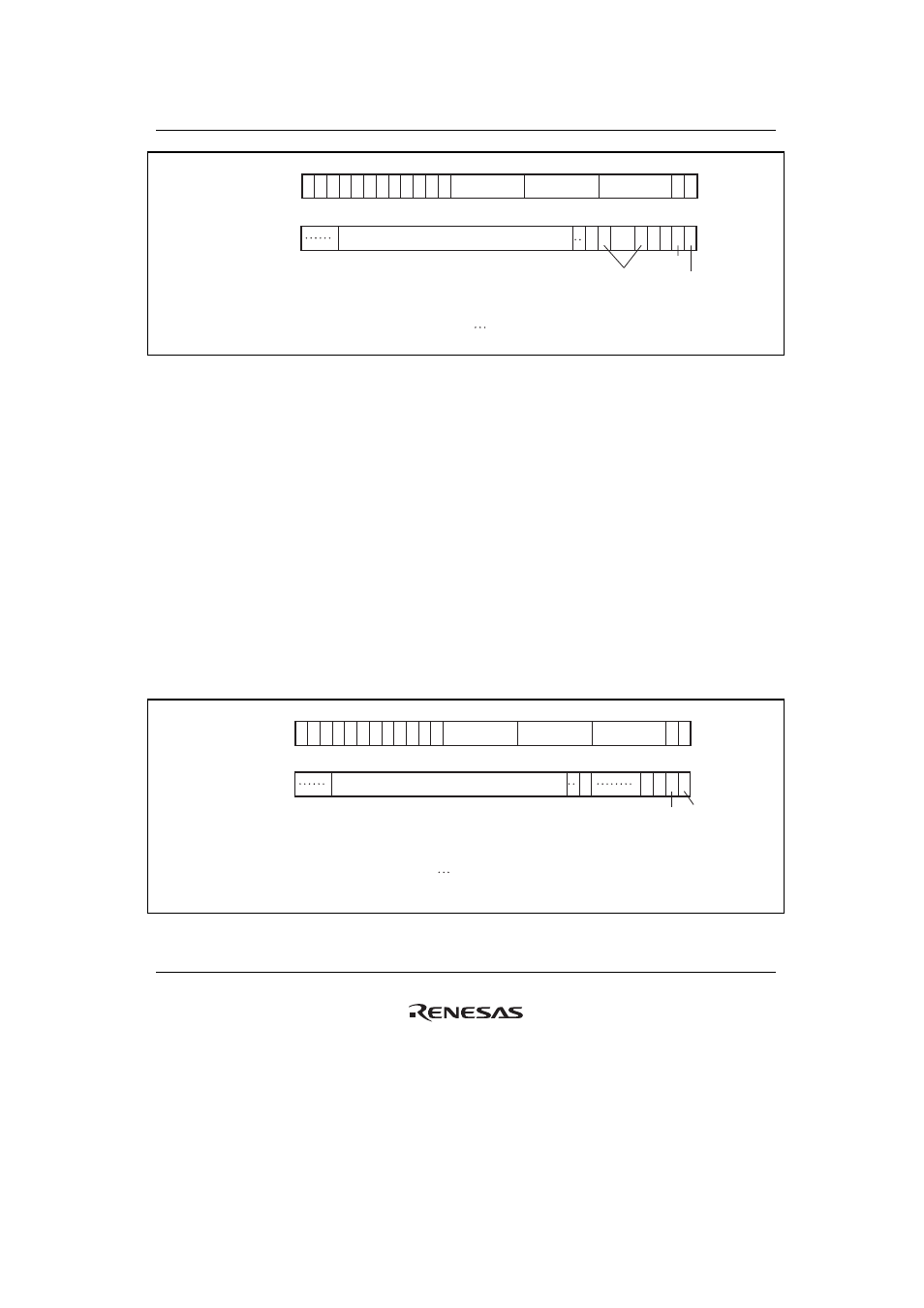
7.7.6
UTLB Data Array (TLB Extended Mode)
In TLB extended mode, the names of the data arrays have been changed from UTLB data array to
UTLB data array 1, UTLB data array 2 is added, and the EPR and ESZ bits are accessible. In TLB
extended mode, the PR and SZ bits of UTLB data array 1 are reserved and 0 should be specified
as the write value for these bits. In addition, when a write to UTLB data array 1 is performed, a
write to UTLB data array 2 of the same entry should always be performed after that.
In TLB compatible mode (MMUCR.ME
= 0), UTLB data array 2 cannot be accessed. Operation if
they are accessed is not guaranteed.
(1)
UTLB Data Array 1
In TLB extended mode, bits 7 to 4 in the data field, which correspond to the PR and SZ bits in
compatible mode, are reserved. Specify 0 as the write value for these bits.
Legend:
Address field
Data field
PPN:
V:
E:
D:
*:
Physical page number
Validity bit
Entry
Dirty bit
Don't care
C:
SH:
WT:
:
Cacheability bit
Share status bit
Write-through bit
Reserved bits
(write value should be 0,
and read value is undefined)
31
2 1 0
V
10 9 8 7
29 28
2 1
4 3
C D
PPN
31
0
0
0
1 1 1 1 0 1 1 1 0 0 0 0
E
20 19
8 7
14 13
WT
SH
* * * * * *
* *
*
* * *
Figure 7.24 Memory-Mapped UTLB Data Array 1 (TLB Extended Mode)