4 pll control register (pllcr) – Renesas SH7781 User Manual
Page 777
15. Clock Pulse Generator (CPG)
Rev.1.00 Jan. 10, 2008 Page 747 of 1658
REJ09B0261-0100
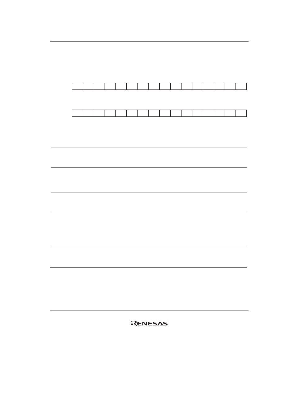
15.4.4
PLL Control Register (PLLCR)
PLLCR is a 32-bit readable/writable register that controls the clock output on the CLKOUT pin.
This register can only be accessed in longwords.
16
17
18
19
20
21
22
23
24
25
26
27
28
29
31
30
0
0
0
0
0
0
0
0
0
0
0
0
0
0
0
0
⎯
⎯
⎯
⎯
⎯
⎯
⎯
⎯
⎯
⎯
⎯
⎯
⎯
⎯
⎯
⎯
R/W
R/W
R/W
R/W
R/W
R/W
R/W
R/W
R
R
R
R
R
R
R
R
BIt:
Initial value:
R/W:
0
1
2
3
4
5
6
7
8
9
10
11
12
13
15
14
0
0
0
0
0
0
0
0
0
0
0
0
0
0
0
0
⎯
CKOFF
⎯
⎯
⎯
⎯
⎯
⎯
⎯
⎯
⎯
⎯
⎯
⎯
⎯
⎯
R
R/W
R
R
R
R
R
R
R
R
R
R
R
R
R
R
BIt:
Initial value:
R/W:
Bit Bit
Name
Initial
Value R/W Description
31 to 24
⎯ 0
R
Reserved
These bits are always read as 0. The write value
should always be 0.
23 to 16
⎯
All 0
R/W
Reserved
These bits are always read as 0. The write value
should always be 0. If a value other than 0 is written,
the operation is not guaranteed.
15 to 2
⎯ All
0
R
Reserved
These bits are always read as 0. The write value
should always be 0.
1
CKOFF
0
R/W
CLKOUT Output Enabled
Stops clock output on the CLKOUT pin
0: Clock is output on the CLKOUT pin
1: The CLKOUT pin is placed in the high impedance
state
0
⎯ 0
R
Reserved
This bit is always read as 0. The write value should
always be 0.