Renesas SH7781 User Manual
Page 228

7. Memory Management Unit (MMU)
Rev.1.00 Jan. 10, 2008 Page 198 of 1658
REJ09B0261-0100
(2)
UTLB Data Array 2
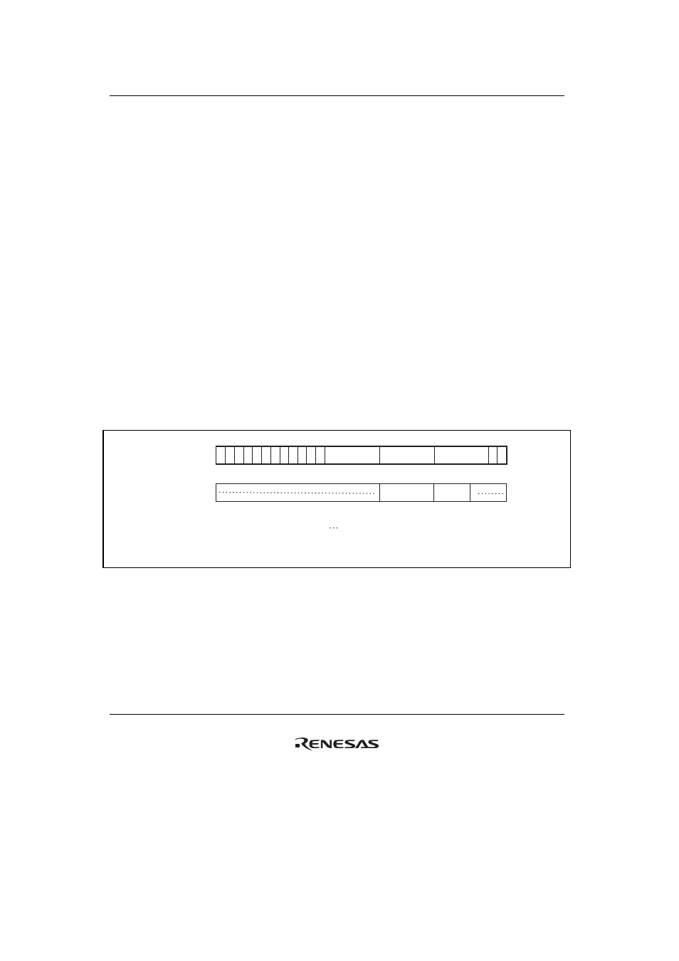
The UTLB data array is allocated to addresses H'F780 0000 to H'F78F FFFF in the P4 area.
Access to data array 2 requires a 32-bit address field specification (when reading or writing) and a
32-bit data field specification (when writing). Information for selecting the entry to be accessed is
specified in the address field, and EPR and ESZ to be written to data array 2 are specified in the
data field.
In the address field, bits [31:20] have the value H'F78 indicating UTLB data array 2 and the entry
is specified by bits [13:8].
In the data field, bits [13:8] indicate EPR, and bits [7:4] indicate ESZ, respectively.
The following two kinds of operation can be applied to UTLB data array 2:
1. UTLB data array 2 read
EPR and ESZ are read into the data field from the UTLB entry corresponding to the entry set
in the address field.
2. UTLB data array 2 write
EPR and ESZ specified in the data field are written to the UTLB entry corresponding to the
entry set in the address field.
Legend:
0 0 0
20 19
Address field
Data field
31
0
EPR
ESZ
8 7
2 1
4 3
31
0
0
0
1 1 1 1 0 1 1 1 1
E
8 7
14 13
13
* * * * * *
* *
*
* * *
E:
EPR:
ESZ:
*:
Entry
Protection key data
Page size bits
Don't care
Reserved bits
(write value should be 0,
and read value is undefined)
:
Figure 7.25 Memory-Mapped UTLB Data Array 2 (TLB Extended Mode)
