3 csn bus control register (csnbcr) – Renesas SH7781 User Manual
Page 401
11. Local Bus State Controller (LBSC)
Rev.1.00 Jan. 10, 2008 Page 371 of 1658
REJ09B0261-0100
11.4.3
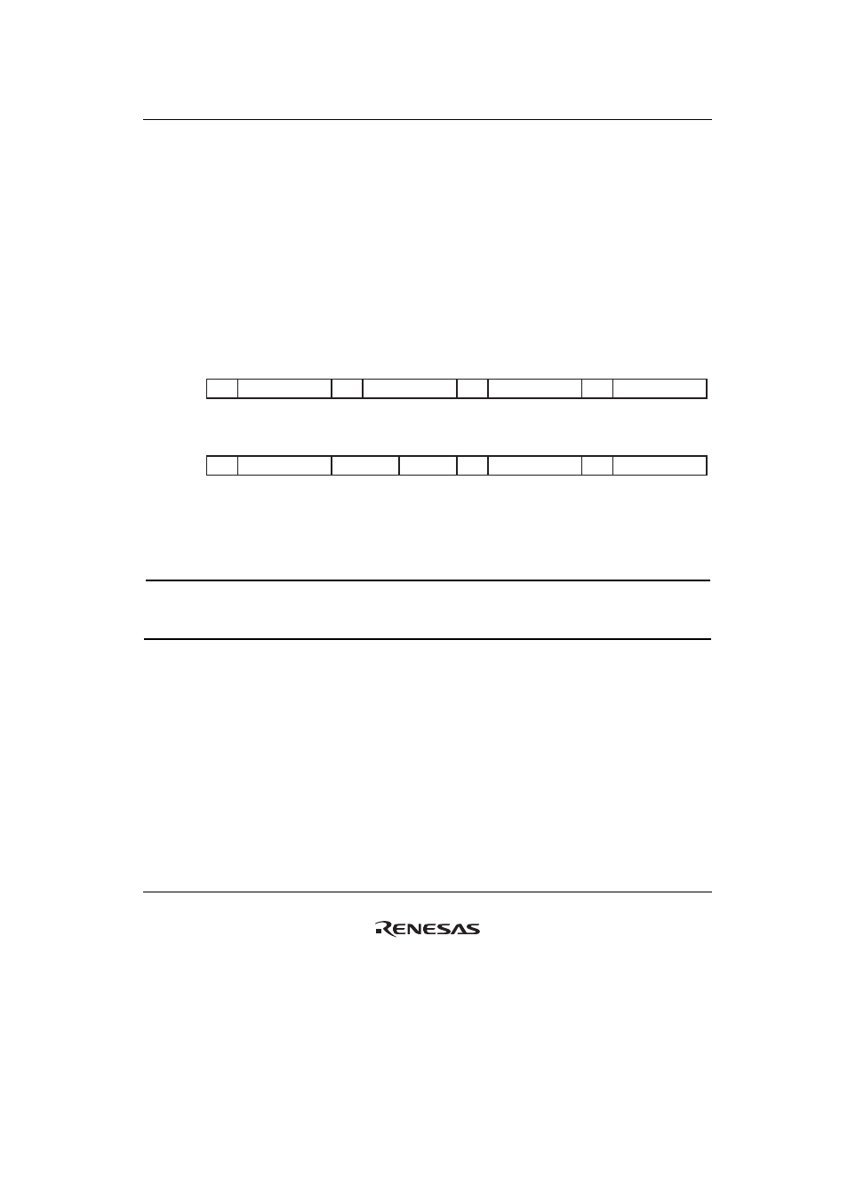
CSn Bus Control Register (CSnBCR)
CSnBCR are 32-bit readable/writable registers that specify the bus width for area n (n
= 0 to 6),
idle mode between cycles, burst ROM setting and memory types.
Some types of memory continue to drive the data bus immediately after the read signal is turned
off. Therefore, data buses may collide with each other when different memory areas are accessed
consecutively or memory writing is performed immediately after it is read. This LSI automatically
inserts idle cycles as specified with CSnBCR when the data buses may collide. In the idle cycles,
CSn, RD, WEn, CE2A, CE2B, BS and R/W are set to high, and the data bus is not driven.
CSnBCR is initialized to H'7777 77F0 at a power-on reset, but is not initialized by a manual reset.
16
17
18
19
20
21
22
23
24
25
26
27
28
29
31
30
1
1
1
0
1
1
1
0
1
1
1
0
1
1
0
1
IWRRD
⎯
IWRWS
⎯
IWRWD
⎯
IWW
⎯
R/W
R/W
R/W
R
R/W
R/W
R/W
R
R/W
R/W
R/W
R
R/W
R/W
R
R/W
BIt:
Initial value:
R/W:
0
1
2
3
4
5
6
7
8
9
10
11
12
13
15
14
0
0
0
0
1
1
1
1
1
1
1
0
1
1
0
1
TYPE
MPX*
BW
RDSPL
SZ*
BST
IWRRS
⎯
R/W
R/W
R/W
R/W*
R/W
R/W
R/W
R/W
R/W*
R/W*
R/W
R/W
R/W
R/W
R
Note: * Bits SZ and MPX in CS0BCR are read-only.
R/W
BIt:
Initial value:
R/W:
Bit Bit
Name
Initial
Value R/W Description
31
⎯ 0
R
Reserved
This bit is always read as 0. The write value should
always be 0.