10 h-udi module signal timing, 0 to 3.6 v, v, 1 v, t – Renesas SH7781 User Manual
Page 1635: 40 to 85°c, c, 30 pf, pll2 on, Figure 32.44 tck input timing
32. Electrical Characteristics
Rev.1.00 Jan. 10, 2008 Page 1605 of 1658
REJ09B0261-0100
32.3.10
H-UDI Module Signal Timing
Table 32.15 H-UDI Module Signal Timing
Conditions: V
DDQ
= 3.0 to 3.6 V, V
DD
= 1.1 V, T
a
=
−40 to 85°C, C
L
= 30 pF, PLL2 on
Item Symbol
Min.
Max. Unit
Figure
Remarks
Input clock cycle
t
TCKcyc
50 — ns
32.44,
32.46
Input clock pulse width (high)
t
TCKH
15 — ns
32.44
Input clock pulse width (low)
t
TCKL
15
—
ns
Input clock rise time
t
TCKr
—
10
ns
Input clock fall time
t
TCKf
—
10
ns
ASEBRK setup time
t
ASEBRKS
10 — t
cyc
32.45
ASEBRK hold time
t
ASEBRKH
1
— ms
TDI/TMS setup time
t
TDIS
15
—
ns
32.46
TDI/TMS hold time
t
TDIH
15
—
ns
TDO data delay time
t
TDO
0 12
ns
ASE-PINBRK pulse width
t
PINBRK
2 — t
Pcyc
32.47
Notes: 1. During a boundary scan, t
TCKcyc
is the period corresponding to a frequency of 10 MHz, i.e.
0.1
μs.
2.
t
cyc
is the period of one CKIO clock cycle.
3.
t
Pcyc
is the period of one peripheral clock (Pck) cycle.
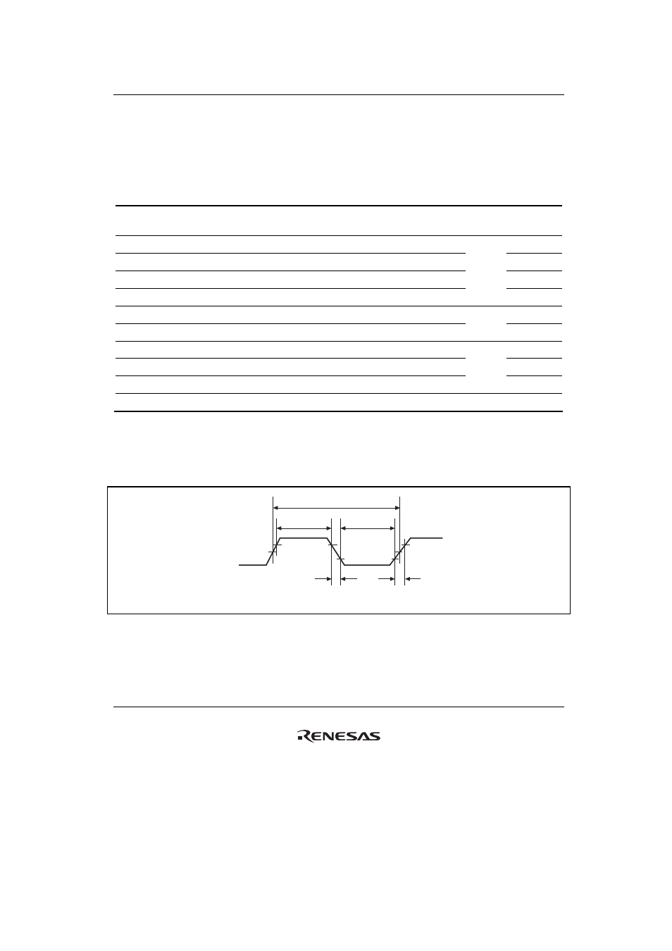
t
TCKH
t
TCKf
t
TCKr
t
TCKL
t
TCKcyc
V
IH
V
IH
V
IH
1/2V
DDQ
1/2V
DDQ
V
IL
V
IL
Note: When the clock is input from the TCK pin.
Figure 32.44 TCK Input Timing