Renesas SH7781 User Manual
Page 1493
29. User Break Controller (UBC)
Rev.1.00 Jan. 10, 2008 Page 1463 of 1658
REJ09B0261-0100
29.2.2
Match Operation Setting Registers 0 and 1 (CRR0 and CRR1)
CRR0 and CRR1 are readable/writable 32-bit registers which specify the operation to be executed
when channels 0 and 1 satisfy the match condition, respectively. The following operations can be
set in the CRR0 and CRR1 registers: (1) breaking at a desired timing for the instruction fetch cycle
and (2) requesting a break.
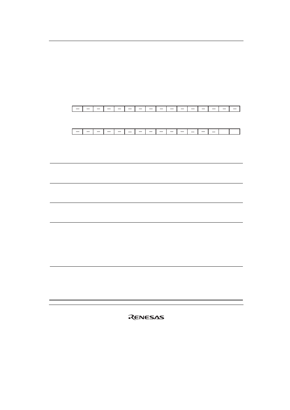
• CRR0
31
30
29
28
27
26
25
24
23
22
21
20
19
18
17
16
0
0
0
0
0
0
0
0
0
0
0
0
0
0
0
0
PCB
BIE
R
R
R
R
R
R
R
R
R
R
R
R
R
R
R
R
15
14
13
12
11
10
9
8
7
6
5
4
3
2
1
0
0
0
1
0
0
0
0
0
0
0
0
0
0
0
0
0
R
R
R
R
R
R
R
R
R
R
R
R
R
R
R/W
R/W
Bit :
Initial value :
R/W:
Bit :
Initial value :
R/W:
Bit Bit
Name
Initial
Value R/W
Description
31 to 14 —
All 0
R
Reserved
For read/write in this bit, refer to General Precautions
on Handling of Product.
13 —
1 R
Reserved
This bit is always read as 1. The write value should
always be 1.
12 to 2
—
All 0
R
Reserved
For read/write in this bit, refer to General Precautions
on Handling of Product.
1
PCB
0
R/W
PC Break Select
Specifies either before or after instruction execution as
the break timing for the instruction fetch cycle. This bit
is invalid for breaks other than the ones for the
instruction fetch cycle.
0: Sets the PC break before instruction execution.
1: Sets the PC break after instruction execution.
0 BIE 0 R/W
Break
Enable
Specifies whether or not to request a break when the
match condition is satisfied for the channel.
0: Does not request a break.
1: Requests a break.