7 transfer clock control register (clkon) – Renesas SH7781 User Manual
Page 1223
24. Multimedia Card Interface (MMCIF)
Rev.1.00 Jan. 10, 2008 Page 1193 of 1658
REJ09B0261-0100
24.3.7
Transfer Clock Control Register (CLKON)
CLKON controls the transfer clock frequency and clock ON/OFF.
At this time, use a sufficiently slow clock for transfer through open-drain type output in MMC
mode.
In a command sequence, do not perform clock ON/OFF or frequency modification.
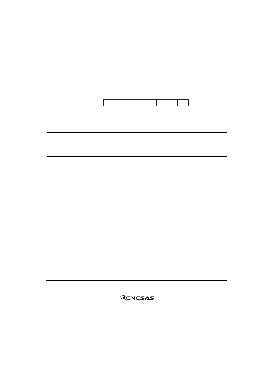
Bit:
Initial value:
R/W:
7
6
5
4
3
2
1
0
0
0
0
0
0
0
0
0
R/W
CLKON
CSEL2 CSEL1 CSEL0
R
R
R
R/W
R/W
R/W
R/W
⎯
⎯
⎯
CSEL3
Bit Bit
Name
Initial
Value R/W Description
7 CLKON
0 R/W
Clock
On
0: Stops the transfer clock output from the MMCCLK
pin.
1: Outputs the transfer clock from the MMCCLK pin.
6 to 4
—
All 0
R
Reserved
These bits are always read as 0. The write value
should always be 0.
3
2
1
0
CSEL3
CSEL2
CSEL1
CSEL0
0
0
0
0
R/W
R/W
R/W
R/W
Transfer Clock Frequency Select
0000: Reserved
0001: Uses the 1/2-divided peripheral clock (Pck) as a
transfer clock.
0010: Uses the 1/4-divided peripheral clock as a
transfer clock.
0011: Uses the 1/8-divided peripheral clock as a
transfer clock.
0100: Uses the 1/16-divided peripheral clock as a
transfer clock.
0101: Uses the 1/32-divided peripheral clock as a
transfer clock.
0110: Uses the 1/64-divided peripheral clock as a
transfer clock.
0111: Uses the 1/128-divided peripheral clock as a
transfer clock.
1000: Uses the 1/256-divided peripheral clock as a
transfer clock.
1001 to 1111: Setting prohibited