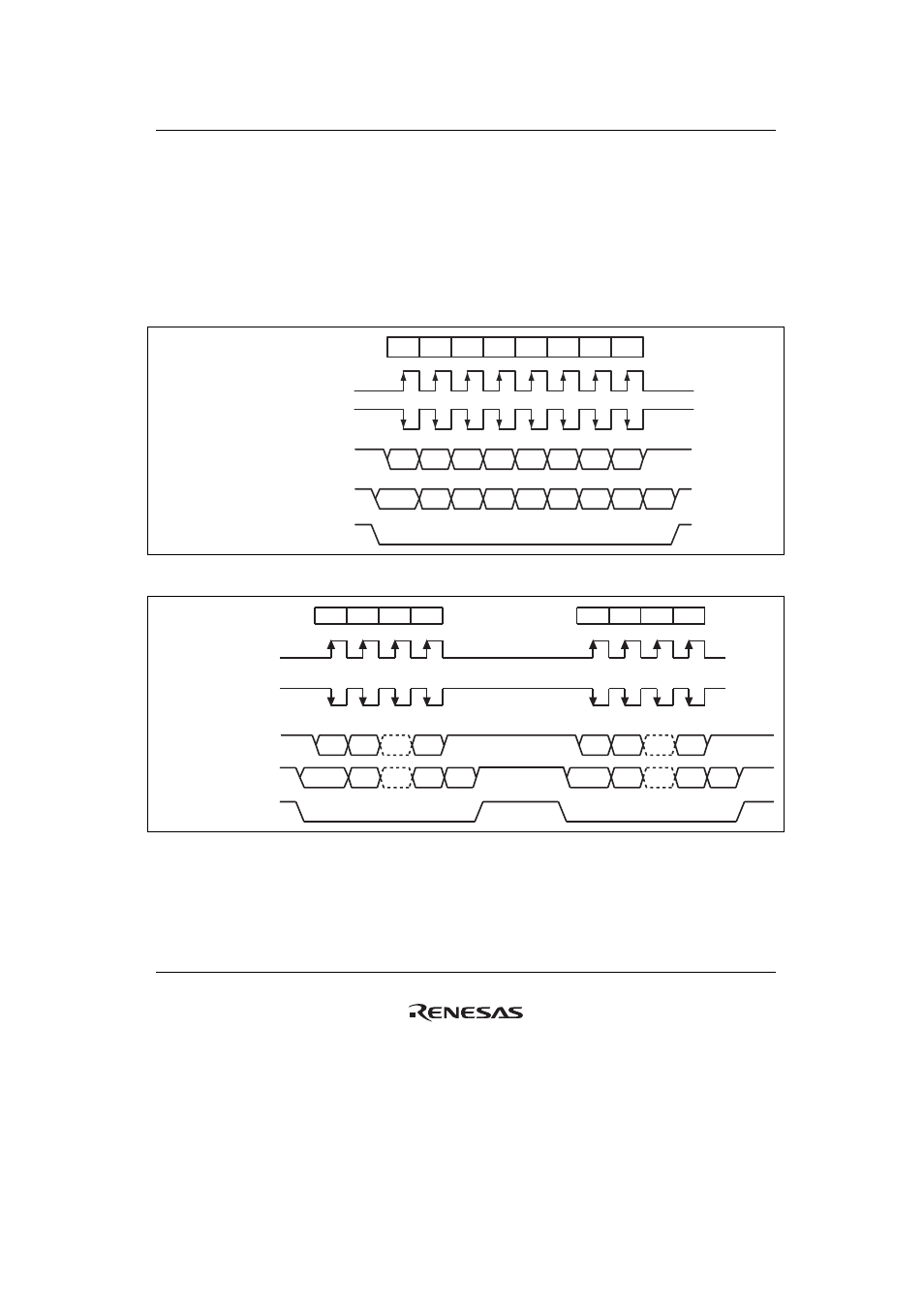
3 timing diagrams, Figure 23.3 timing conditions when fbs = 0 – Renesas SH7781 User Manual
Page 1197

23. Serial Peripheral Interface (HSPI)
Rev.1.00 Jan. 10, 2008 Page 1167 of 1658
REJ09B0261-0100
23.4.3
Timing Diagrams
The following diagrams explain the timing relationship of all shift and sample processes in the
HSPI. Figure 23.3 shows the conditions when FBS = 0, figure 23.4 shows the conditions when
FBS = 0 (continuous transfer), figure 23.5 shows the conditions when FBS = 1, and figure 23.6
shows the conditions when FBS = 1 (continuous transfer). It can be seen that if CLKP in SPCR is
0, transmit data is shifted at the falling edge of HSPI_CLK and receive data is sampled at the
rising edge of HSPI_CLK. The opposite is true when CLKP = 1.
Data transfer cycle
HSPI_CLK (CLKP = 0)
HSPI_CLK (CLKP = 1)
1
4
3
2
8
7
6
5
HSPI_TX
MSB
6
5
4
3
2
1
LSB
MSB
6
5
4
3
2
1
LSB
*
HSPI_RX
HSPI_CS
Figure 23.3 Timing Conditions when FBS = 0
HSPI_CLK (CLKP = 0)
HSPI_CLK (CLKP = 1)
1
8
..
2
9
16
..
10
HSPI_TX
MSB
6
LSB
MSB
6
LSB
MSB
6
LSB
MSB
6
LSB
*
HSPI_RX
HSPI_CS
Data transfer cycle
*
Figure 23.4 Timing Conditions when FBS = 0 (Continuous Transfer)
