Renesas SH7781 User Manual
Page 280
9. On-Chip Memory
Rev.1.00 Jan. 10, 2008 Page 250 of 1658
REJ09B0261-0100
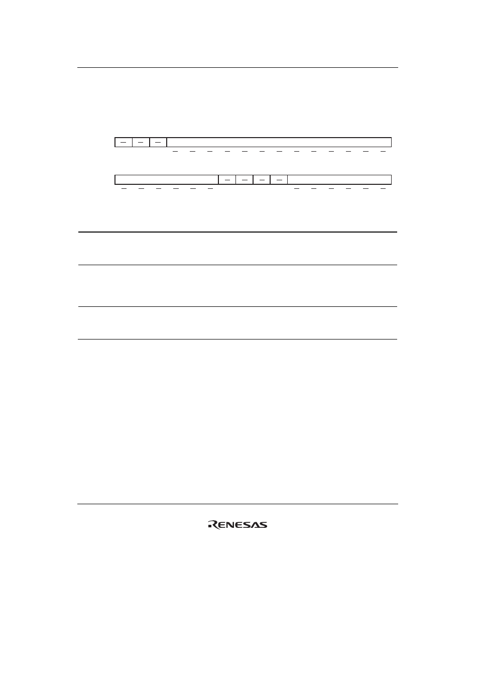
9.2.3
OL memory Transfer Source Address Register 1 (LSA1)
When MMUCR.AT = 0 or RAMCR.RP = 0, the LSA1 specifies the transfer source physical
address for block transfer to page 1A or 1B in the OL memory.
31
30
29
28
27
26
25
24
23
22
21
20
19
18
17
16
Bit :
0
0
0
Initial value :
R
R
R
R/W
R/W
R/W
R/W
R/W
R/W
R/W
L1SADR
L1SADR
L1SSZ
R/W
R/W
R/W
R/W
R/W
R/W
R/W:
15
14
13
12
11
10
9
8
7
6
5
4
3
2
1
0
Bit :
0
0
0
0
Initial value :
R/W
R/W
R/W
R/W
R/W
R/W
R
R
R
R
R/W
R/W
R/W
R/W
R/W
R/W
R/W:
Bit Bit
Name
Initial
Value R/W
Description
31 to 29 —
All 0
R
Reserved
For read/write in these bits, refer to General
Precautions on Handling of Product.
28 to 10 L1SADR
Undefined R/W
OL memory Page 1 Block Transfer Source Address
When MMUCR.AT = 0 or RAMCR.RP = 0, these bits
specify transfer source physical address for block
transfer to page 1A or 1B in the OL memory.
9 to 6
—
All 0
R
Reserved
For read/write in these bits, refer to General
Precautions on Handling of Product.
- Single-Chip Microcomputer M34551T2-MCU (42 pages)
- M3T-FLX-80NRA (6 pages)
- 70 (162 pages)
- M16C/30P (102 pages)
- PROM Programming Adapter PCA7427G02 (20 pages)
- R0E572110CFK00 (40 pages)
- H8/325 Series (20 pages)
- Single-Chip Microcomputer H8/36079 (27 pages)
- Direct Dummy IC M3T-DIRECT100S (4 pages)
- M3A-2152 (95 pages)
- PCA7755D (6 pages)
- M16C/6N5 (106 pages)
- SH7085 (50 pages)
- QFP-144 (23 pages)
- H8/3834 Series (22 pages)
- RSKM16C62P (3 pages)
- H8/33937 (22 pages)
- Single-Chip Microcomputer H8SX/1622 (5 pages)
- E6000 (29 pages)
- PCA7400 (18 pages)
- PCA4738FF-64 (20 pages)
- SuperH HS7339KCU01HE (43 pages)
- M16C FAMILY (103 pages)
- PCA7412F-100 (20 pages)
- 4513 (210 pages)
- M34551E8FP (16 pages)
- Dummy IC M3T-SSOP36B-450 (4 pages)
- Emulation Pod M30100T3-RPD-E (52 pages)
- Converter Board for M30102 M30102T-PTC (4 pages)
- SH7145 (31 pages)
- HS1653ECN61H (36 pages)
- Converter Board R0E521276CFG00 (4 pages)
- PCA7302E1F-80 (18 pages)
- H8/3814 Series (21 pages)
- H8S/2646 Series (20 pages)
- SuperHTM Family SH7125 Series (40 pages)
- M30262T-PTC (4 pages)
- SH7670 (82 pages)
- H8/3864 Series (20 pages)
- Emulator System M3T-MR100 (306 pages)
- 38K0 (6 pages)
- PLQP0176KB-A (40 pages)
- Direct Dummy IC M3T-DIRECT80S (6 pages)
- PCA4738L-80A (26 pages)
- Converter Board R0E5212BACFG00 (6 pages)