Renesas SH7781 User Manual
Page 646
13. PCI Controller (PCIC)
Rev.1.00 Jan. 10, 2008 Page 616 of 1658
REJ09B0261-0100
Bit Bit
Name
Initial
Value R/W
Description
1 PMD1M
0
SH:
R/W
PCI:
⎯
PCI Power Management D1 Status Transition
Interrupt Mask
0: PMD1 disabled (masked)
1: PMD1 enabled (not masked)
0 PMD0M
0
SH:
R/W
PCI:
⎯
PCI Power Management D0 Status Transition
Interrupt Mask
0: PMD0 disabled (masked)
1: PMD0 enabled (not masked)
(16)
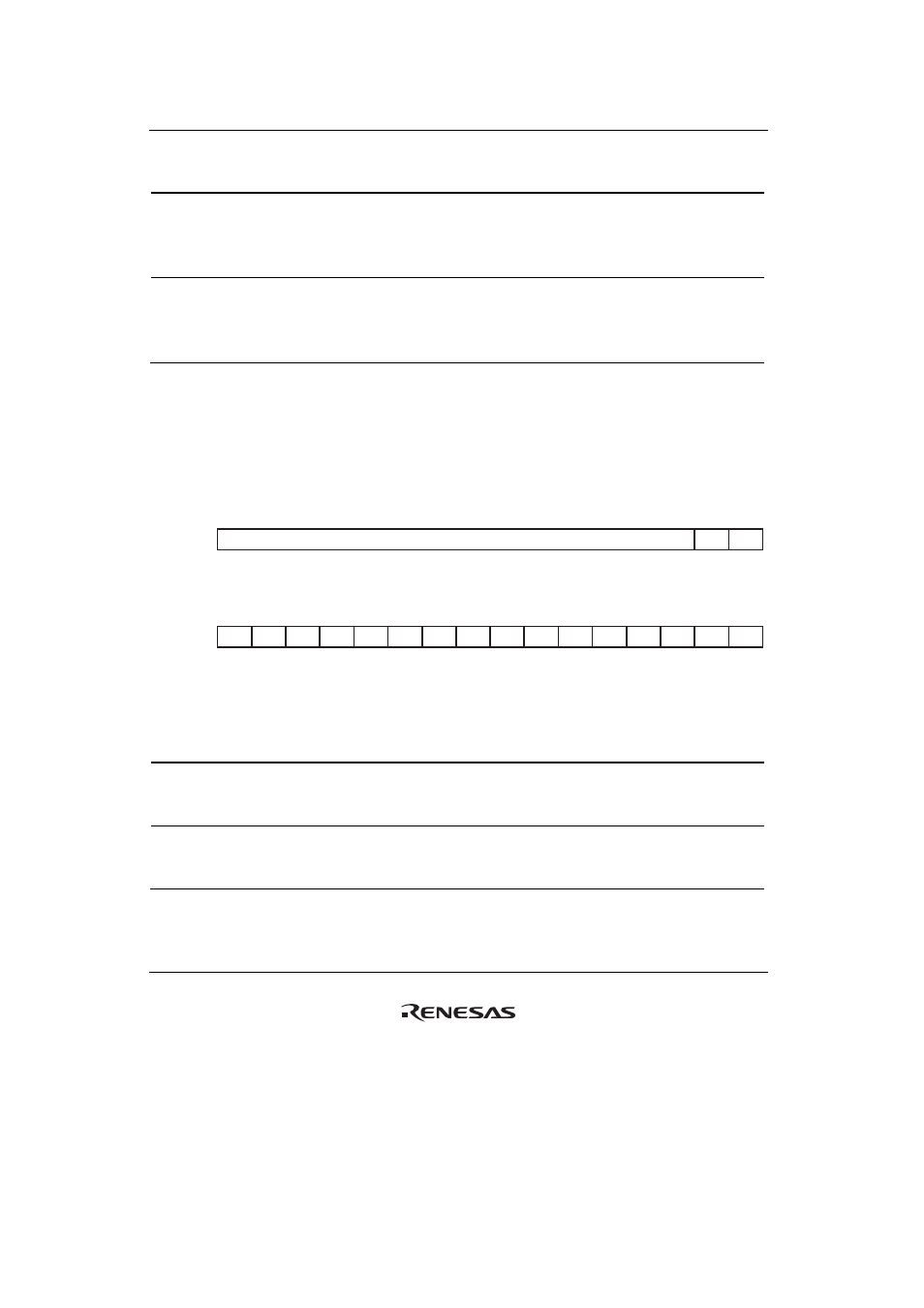
PCI Memory Bank Register 0 (PCIMBR0)
This register specifies the upper 14 bits of the memory space address on the PCI bus for a memory
read or write to the PCI memory space 0 by the CPU or DMAC.
See section 13.4.3 (2), Accessing PCI Memory Space.
SH R/W:
PCI R/W:
SH R/W:
PCI R/W:
16
17
18
19
20
21
22
23
24
25
26
27
28
29
31
30
Bit:
Initial value:
R
R
R/W
R/W
R
R
R
R
R/W
R/W
R/W
R/W
R/W
R/W
R/W
R/W
R/W
R/W
R/W
R/W
0
0
0
0
0
0
0
0
0
0
0
0
0
0
0
0
—
—
PMSBA0
—
—
—
—
—
—
—
—
—
—
—
—
—
—
—
—
—
—
—
—
—
—
—
—
—
—
—
—
—
—
—
—
—
—
—
—
R
R
R
R
R
R
R
R
R
R
R
R
0
0
0
0
0
0
0
0
0
0
0
0
0
0
0
0
—
—
—
—
—
—
—
—
—
—
—
—
0
1
2
3
4
5
6
7
8
9
10
11
12
13
15
14
Bit:
Initial value:
Bit Bit
Name
Initial
Value R/W
Description
31 to 18 PMSBA0
H'0000 SH: R/W
PCI:
⎯
PCI Memory Space 0 Bank Address (14 bits)
These bits specify an bank address for the PCI
memory space 0 for PIO transfer.
17 to 0
⎯
All 0
SH: R
PCI:
⎯
Reserved
These bits are always read as 0. The write value
should always be 0.