6 notes on using 32-bit address extended mode – Renesas SH7781 User Manual
Page 234
7. Memory Management Unit (MMU)
Rev.1.00 Jan. 10, 2008 Page 204 of 1658
REJ09B0261-0100
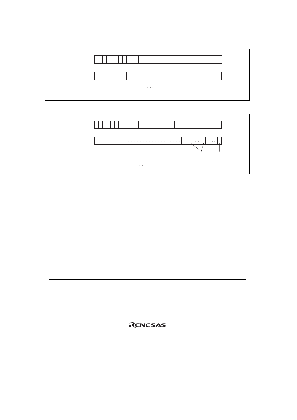
Address field
Data field
VPN:
V:
E:
Physical page number
Validity bit
Entry
: Reserved bits (write value should be 0
and read value is undefined )
31
0
V
8
8 7
VPN
31
19
20
0
1 1 1 1 0
0 0 0
1 1 0
1
0 0
E
23
24
12 11
0 0 0 0 0
0 0 0 0 0
0 0 0
0
Figure 7.28 Memory-Mapped PMB Address Array
Address field
Data field
PPN:
V:
E:
SZ:
Physical page number
Validity bit
Entry
Page size bits
UB:
C:
WT:
:
Buffered write bit
Cacheability bit
Write-through bit
Reserved bits (write value should be 0
and read value is undefined )
31
2 1 0
V
UB
10 9 8 7
4 3
6 5
C
PPN
31
0
1 1 1 1 0 1 1 1 0 0 0 1
E
23
24
19
20
8 7
12 11
SZ
WT
0 0 0 0 0 0 0 0
0 0 0 0 0 0 0 0
Figure 7.29 Memory-Mapped PMB Data Array
7.8.6
Notes on Using 32-Bit Address Extended Mode
When using 32-bit address extended mode, note that the items described in this section are
extended or changed as follows.
(1)
PASCR
The SE bit is added in bit 31 in the control register (PASCR). The bits 6 to 0 of the UB in the
PASCR are invalid (Note that the bit 7 of the UB is still valid). When writing to the P1 or P2 area,
the UB bit in the PMB controls whether a buffered write is performed or not. When the MMU is
enabled, the UB bit in the TLB controls writing to the P0, P3, or U0 area. When the MMU is
disabled, writing to the P0, P3, or U0 area is always performed as a buffered write.
Bit Bit
Name
Initial
Value R/W
Description
31
SE
0
R/W
0: 29-bit address mode
1: 32-bit address extended mode