2 itlb data array (tlb compatible mode) – Renesas SH7781 User Manual
Page 222

7. Memory Management Unit (MMU)
Rev.1.00 Jan. 10, 2008 Page 192 of 1658
REJ09B0261-0100
7.7.2
ITLB Data Array (TLB Compatible Mode)
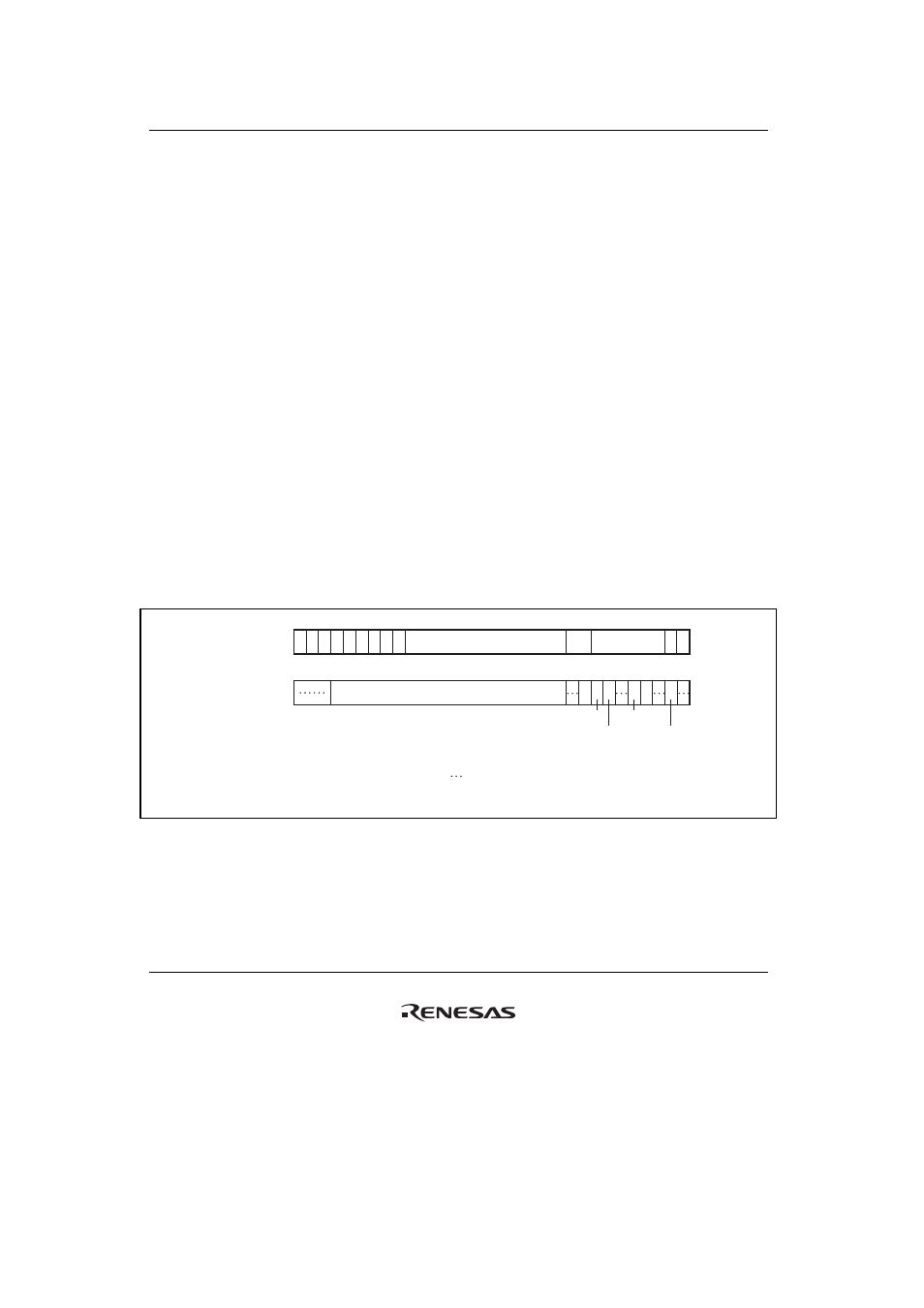
The ITLB data array is allocated to addresses H'F300 0000 to H'F37F FFFF in the P4 area. A data
array access requires a 32-bit address field specification (when reading or writing) and a 32-bit
data field specification (when writing). Information for selecting the entry to be accessed is
specified in the address field, and PPN, V, SZ, PR, C, and SH to be written to the data array are
specified in the data field.
In the address field, bits [31:23] have the value H'F30 indicating ITLB data array and the entry is
specified by bits [9:8].
In the data field, bits [28:10] indicate PPN, bit [8] indicates V, bits [7] and [4] indicate SZ, bit [6]
indicates PR, bit [3] indicates C, and bit [1] indicates SH.
The following two kinds of operation can be used on ITLB data array:
1. ITLB data array read
PPN, V, SZ, PR, C, and SH are read into the data field from the ITLB entry corresponding to
the entry set in the address field.
2. ITLB data array write
PPN, V, SZ, PR, C, and SH specified in the data field are written to the ITLB entry
corresponding to the entry set in the address field.
Address field
31
23
0
1 1 1 1 0 0
0 0
0
1 1
E
Data field
PPN:
V:
E:
SZ[1:0]:
*:
24
Physical page number
Validity bit
Entry
Page size bits
Don't care
10 9 8 7
2 1
PR:
C:
SH:
:
Protection key data
Cacheability bit
Share status bit
Reserved bits (write value should be 0,
and read value is undefined )
31
2 1 0
V
10 9 8 7
30 29 28
4 3
6 5
SZ1
SZ0
SH
PR
C
PPN
* * * * * * * * * * * *
* * * * * *
Figure 7.19 Memory-Mapped ITLB Data Array (TLB Compatible Mode)
