Renesas SH7781 User Manual
Page 1018
20. Graphics Data Translation Accelerator (GDTA)
Rev.1.00 Jan. 10, 2008 Page 988 of 1658
REJ09B0261-0100
20.3.10
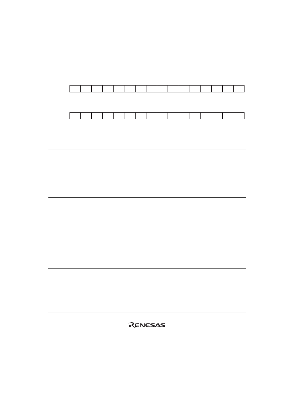
GA Buffer RAM 0 Data Alignment Register (DCP_CTL)
DCP_CTL is in the GDTA common register block and specifies data alignment of the data stored
in buffer RAM 0.
16
17
18
19
20
21
22
23
24
25
26
27
28
29
31
30
0
0
0
0
0
0
0
0
0
0
0
0
0
0
0
0
⎯
⎯
⎯
⎯
⎯
⎯
⎯
⎯
⎯
⎯
⎯
⎯
⎯
⎯
⎯
⎯
⎯
⎯
⎯
⎯
⎯
⎯
⎯
⎯
⎯
⎯
⎯
⎯
⎯
⎯
⎯
⎯
BIt:
Initial value:
R/W:
0
1
2
3
4
5
6
7
8
9
10
11
12
13
15
14
0
0
0
0
0
0
0
0
0
0
0
0
0
0
0
0
DCP_DTUA
DCP_DTSA
DCP_
DTAM
⎯
⎯
⎯
⎯
⎯
⎯
⎯
⎯
⎯
⎯
⎯
R/W
R/W
R/W
R/W
R/W
⎯
⎯
⎯
⎯
⎯
⎯
⎯
⎯
⎯
⎯
⎯
BIt:
Initial value:
R/W:
Bit Bit
Name
Initial
Value R/W Description
31 to 5
⎯ All
0
⎯ Reserved
These bits are always read as 0. The write value should
always be 0.
4
DCP_DTAM
0
R/W
Specifies data alignment conversion mode
0: Data alignment is performed using an endian signal
1: Data alignment is performed using the DCP_CTL
register setting
3, 2
DCP_DTSA
0
R/W
Specifies the data size for data alignment conversion.
00: No conversion
01: 64 bits
10: 32 bits
11: 16 bits
1, 0
DCP_DTUA
0
R/W
Specifies the unit for data alignment conversion.
00: No conversion
01: 8 bits
10: 16 bits
11: 32 bits
Note: For details of data alignment conversion patterns, refer to section 20.6, Data Alignment.