2 gdta address space – Renesas SH7781 User Manual
Page 1003
20. Graphics Data Translation Accelerator (GDTA)
Rev.1.00 Jan. 10, 2008 Page 973 of 1658
REJ09B0261-0100
20.2
GDTA Address Space
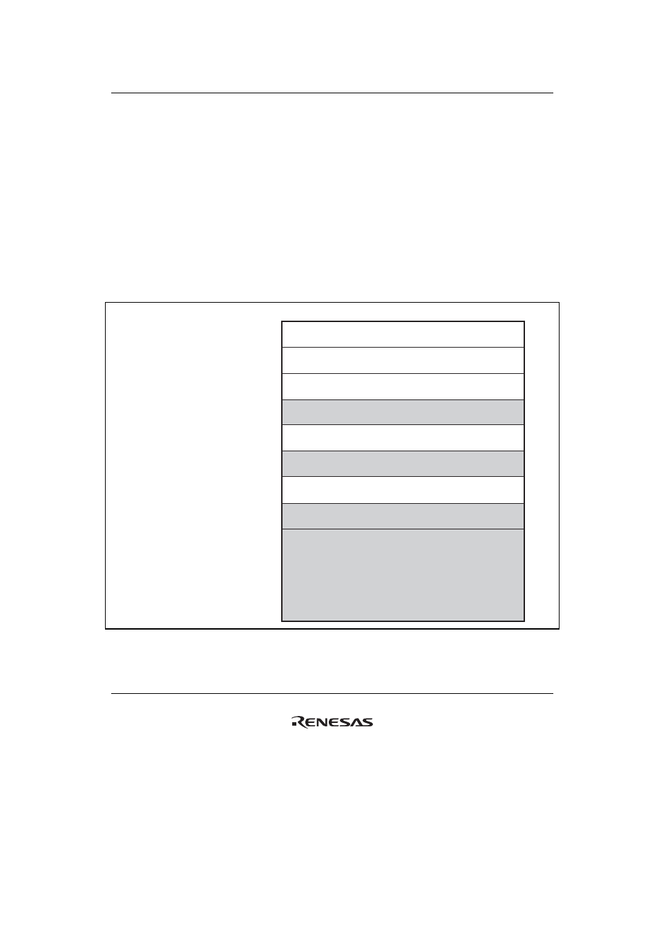
Figure 20.2 shows the GDTA address space (physical addresses). The GDTA consists of a number
of function blocks; the address space is divided into function block units owned by the respective
blocks. However, not all actually existing addresses are on the space; addresses following those in
a function block are mapped as mirror spaces for the function block. For the details of addresses
actually existing in each function block, refer to section 20.3, Register Descriptions. Mirror spaces
also exist in buffer RAM.
Note: The space from H'FE40_3000 to H'FE40_3FFF, excluding the space for registers
DRCL_CTL, DWCL_CTL, DRMC_CTL, DWMC_CTL, DCP_CTL, and DID_CTL is a
reserved area, and write access is prohibited. If write access is made, correct operation
cannot be guaranteed.
Common registers for bus interface
CL
MC
Buffer RAM 0 (8 Kbytes)
Buffer RAM 1 (8 Kbytes)
Reserved
Undefined (buffer RAM 0 mirror space: 8 Kbytes
× 7)
Undefined (buffer RAM 1 mirror space: 8 Kbytes
× 7)
Reserved
P4 area address
Area 7 address
H'FE40 0000
H'1E40 0000
H'FE40 1000
H'1E40 1000
H'FE40 2000
H'1E40 2000
H'FE40 3000
H'1E40 3000
H'FE41 0000
H'1E41 0000
H'FE41 2000
H'1E41 2000
H'FE42 0000
H'1E42 0000
H'FE42 2000
H'1E42 2000
H'FE43 0000
H'1E43 0000
H'FE4F FFFF
H'1E4F FFFF
Figure 20.2 GDTA Address Space Map (Physical Addresses)