Transceiver pll signals, Transceiver pll signals -4 – Altera Transceiver PHY IP Core User Manual
Page 593
Name
Value
Description
Reference clock frequency
Variable
Specifies the frequency of the PLL input
reference clock. The PLL must generate an
output frequency that equals the Base data
rate/2. You can use any Input clock
frequency that allows the PLLs to generate
this output frequency.
Selected reference clock source
0-4
Specifies the index of the TX reference clock
for the initial configuration of the TX PLL.
Logical index 0 corresponds to TX reference
clock 1, and so on.
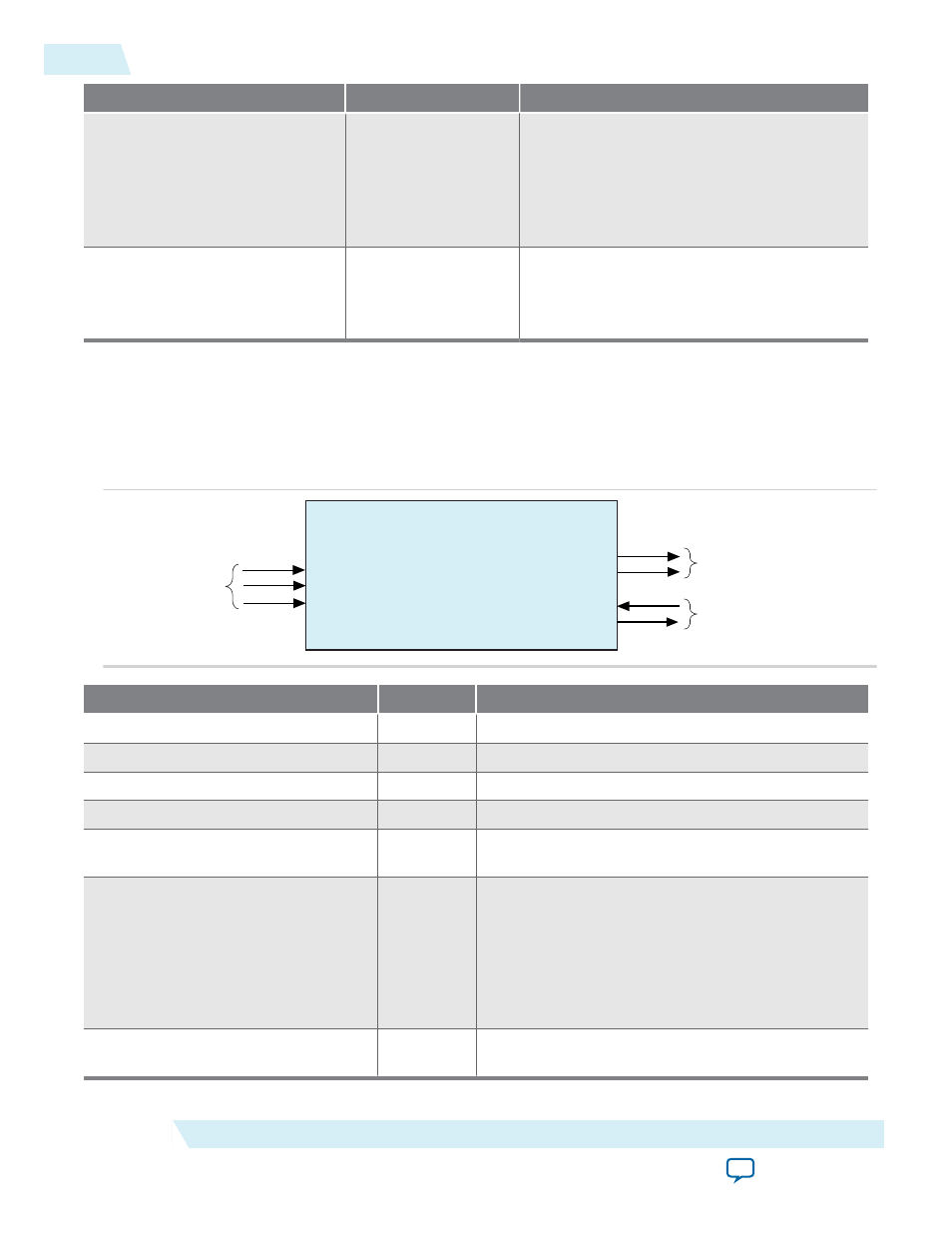
Transceiver PLL Signals
Figure 18-2: Transceiver PLL Top-Level Signals
The following figure illustrates the top-level signals of the Transceiver PLL which are defined in the table
below.
pll_powerdown
pll_refclk[
-1:0]
pll_fbclk
pll_clkout
pll_locked
reconfig_to_xcvr[69:0]
reconfig_from_xcvr[45:0]
Transceiver PLL Top-Level Signals
PLL Clock
and Status
PLL
Inputs
Dynamic
Reconfiguration
(optional)
Signal Name
Direction
Description
pll_powerdown
Input
When asserted, powers down the PLL.
pll_refclk
Input
Input reference clock for the CMU PLL.
pll_fbclk
Input
The feedback input port for the PLL.
pll_clkout
Output
Output clock from the PLL.
pll_locked
Output
When asserted, indicates that the PLL has locked to
the input reference clock.
reconfig_to_xcvr[69:0]
Input
Reconfiguration signals from the Transceiver
Reconfiguration Controller. When you enable the
reconfiguration bus, the simulation model for the
TX PLL supports dynamic reconfiguration. When
you enable this bus, the Quartus II software does
not merge TX PLL by default; however, you can
merge TX PLLs using QSF settings.
reconfig_from_xcvr[45:0]
Output
Reconfiguration signals to the Transceiver Reconfi‐
guration Controller.
18-4
Transceiver PLL Signals
UG-01080
2015.01.19
Altera Corporation
Transceiver PLL IP Core for Stratix V, Arria V, and Arria V GZ Devices