6 mcc configuration registers (mccfx), Figure 28-17. si mcc configuration register (mccf), Table 28-15. mccf field descriptions – Freescale Semiconductor MPC8260 User Manual
Page 881: Mcc configuration registers (mccfx) -33, Si mcc configuration register (mccf) -33, Mccf field descriptions -33, Section 28.6, Mcc configuration registers (mccfx), Bed in, Section 28.6, “mcc configuration
Multi-Channel Controllers (MCCs)
MPC8260 PowerQUICC II Family Reference Manual, Rev. 2
Freescale Semiconductor
28-33
Figure 28-16. Receiver Super Channel without Slot Synchronization Example
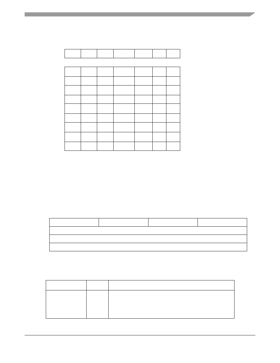
28.6
MCC Configuration Registers (MCCF
x)
The MCC configuration register (MCCF), shown in
, defines the mapping of the MCC
channels to the TDM channels. MCC1 can be connected to SI1 and MCC2 can be connected to SI2. For
each MCCx-SIx pair, each of the four 32 channels subgroups can be connected to one of the four TDM
highways (TDMA, TDMB, TDMC, and TDMD).
0
1
2
3
4
5
6
7
Field
Group 1
Group 2
Group 3
Group 4
Reset
0000_0000
R/W
R/W
Addr
0x0x11B38 (MCCF1), 0x0x11B58 (MCCF2)
Figure 28-17. SI MCC Configuration Register (MCCF)
Table 28-15. MCCF Field Descriptions
Bits Name
Description
0–1, 2–3, 4–5, 6–7
GROUP
x
Group x of channels is used by TDM y as shown in
00 Group x is used by TDM A.
01 Group x is used by TDM B.
10 Group x is used by TDM C.
11 Group x is used by TDM D.
0
1
2
3–10
11–13
14
15
MCC
LOOP SUPER
MCSEL
CNT
BYT
LST
SI RAM Address
1
0
0
0x0
0x0
1
0
Regular Channel
1
0
0
0x1
0x0
1
0
Super Channel 1
1
0
0
0x2
0x0
1
0
Super Channel 2
1
0
0
0x2
0x0
1
0
Super Channel 2
1
0
0
0x2
0x0
1
0
Super Channel 2
1
0
0
0x5
0x0
1
0
Regular Channel
1
0
0
0x1
0x0
1
0
Super Channel 1
1
0
0
0x1
0x0
1
0
Super Channel 1
1
0
0
0x8
0x0
1
1
Regular Channel
The super channel BD tables are associated with channels 1 and 2
SI RAM