Table 15-6. sixrsr field descriptions, 4 si command register (sixcmdr), Figure 15-19. si command register (sixcmdr) – Freescale Semiconductor MPC8260 User Manual
Page 600: Si command register (sixcmdr) -24, Six ram shadow address registers (sixrsr) -24, Sixrsr field descriptions -24, 4 si command register (si, Cmdr), Table 15-6. describes si x rsr fields
Serial Interface with Time-Slot Assigner
MPC8260 PowerQUICC II Family Reference Manual, Rev. 2
15-24
Freescale Semiconductor
Table 15-6. describes SIxRSR fields.
15.5.4
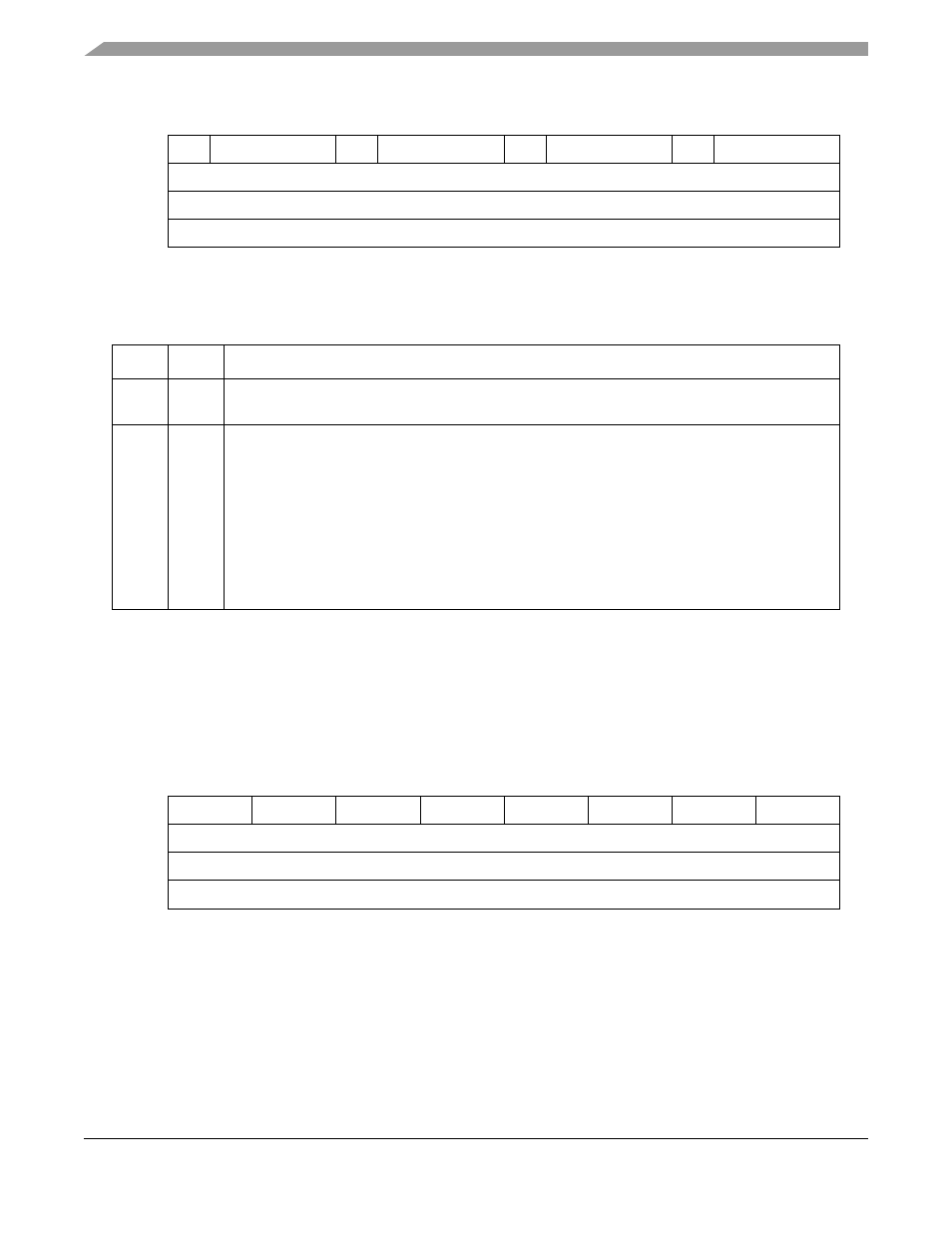
SI Command Register (SI
x
CMDR)
The SI command registers (SIxCMDR), shown in
, allow the user to dynamically program the
SIx RAM. When the user sets bits in the SIxCMDR, the SIx switches to the shadow SIx RAM at the end
of the current-route RAM programming frame. For more information about dynamic programming, see
Section 15.4.5, “Static and Dynamic Routing.”
describes SIxCMDR fields.
0
1
3
4
5
7
8
9
11
12
13
15
Field
—
SSADA
—
SSADB
—
SSADC
—
SSADD
Reset
0000_0000_0000_0000
R/W
R/W
Addr
0x0x11B2E (SI1RSR), 0x0x11B4E (SI2RSR)
Figure 15-18. SI
x RAM Shadow Address Registers (SIxRSR)
Table 15-6. SI
xRSR Field Descriptions
Bits
Name
Description
0, 4, 8,
12
—
Reserved. Should be cleared.
1–3,
5–7,
9–11,
13–15
SSAD
x
Starting bank address for the shadow RAM of TDM a, b, c, or d. Defines the starting bank address
of the shadow SI
x
RAM section that belongs to the corresponding TDM channel.
Note: As noted before, the SI
x
RAM contain four banks of 64 entries for receive and four banks of
64 entries for transmit.
In spite of the above, the starting bank address of each TDM can be programmed by the user in a
granularity of 32 entries, but the user cannot put two different TDMs on the same bank.
The user can put the shadow RAM section of the same TDM on the same bank.
The last entry of a certain TDM frame is determined by the LST bit in the SI
x
RAM entry. The user
must set this bit within the entries of SI
x
RAM shadow blocks for every TDM used. That means
before the starting address of the next TDM.
0
1
2
3
4
5
6
7
Field
CSRRA
CSRTA
CSRRB
CSRTB
CSRRC
CSRTC
CSRRD
CSRTD
Reset
0000_0000
R/W
R/W
Addr
0x0x11B2A (SI1CMDR), 0x0x11B4A (SI2CMDR)
Figure 15-19. SI Command Register (SI
xCMDR)