Chapter 39 i2c controller, Figure 39-1. i2c controller block diagram, C controller – Freescale Semiconductor MPC8260 User Manual
Page 1265: Chapter 39, “i, Chapter 39 i
MPC8260 PowerQUICC II Family Reference Manual, Rev. 2
Freescale Semiconductor
39-1
Chapter 39
I
2
C Controller
The inter-integrated circuit (I
2
C®) controller lets the PowerQUICC II exchange data with other I
2
C
devices, such as microcontrollers, EEPROMs, real-time clock devices, A/D converters, and LCD displays.
The I
2
C controller uses a synchronous, multimaster bus that can connect several integrated circuits on a
board. It uses two signals—serial data (SDA) and serial clock (SCL)—to carry information between the
integrated circuits connected to it.
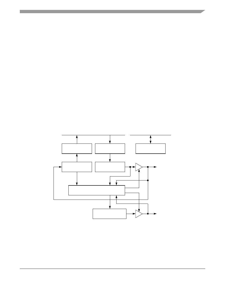
As shown in
, the I
2
C controller consists of transmit and receive sections, an independent
baud-rate generator (BRG), and a control unit. The transmit and receive sections use the same clock, which
is derived from the I
2
C BRG when in master mode and generated externally when in slave mode. Wait
states are inserted during a data transfer if SCL is held low by a slave device. In the middle of a data
transfer, the master I
2
C controller recognizes the need for wait states by monitoring SCL. However, the
I
2
C controller has no automatic time-out mechanism if the slave device does not release SCL; therefore,
software should monitor how long SCL stays low to generate bus timeouts.
Figure 39-1. I
2
C Controller Block Diagram
The I
2
C receiver and transmitter are double-buffered, which corresponds to an effective two-character
FIFO latency. In normal operation, the transmitter shifts the msb (bit 0) out first. When the I
2
C is not
enabled in the I
2
C mode register (I2MOD[EN] = 0), it consumes little power.
Control
Tx Data Register
Rx Data Register
Peripheral Bus
Mode Register
Shift Register
Shift Register
Baud-Rate Generator
SCL
SDA
60x Bus