Figure 28-14. transmitter super channel example, Transmitter super channel example -31, Figure 28-14 – Freescale Semiconductor MPC8260 User Manual
Page 879
Multi-Channel Controllers (MCCs)
MPC8260 PowerQUICC II Family Reference Manual, Rev. 2
Freescale Semiconductor
28-31
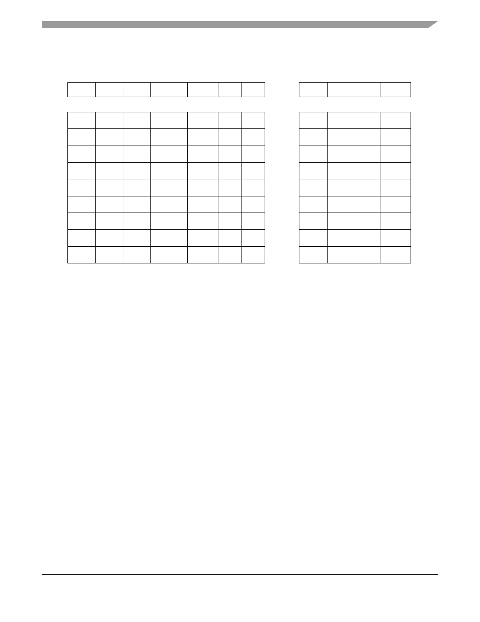
Figure 28-14. Transmitter Super Channel Example
In this example, data is expected to be sent on the first timeslots allocated for each superchannel. Thus for
the first superchannel, timeslot 1 has CNT=0 and BYT=1, the “first byte” condition described in
and the remaining timeslots that are part of this superchannel—timeslots 6 and 7, have
CNT=0x7 and BYT=1. This indicates to the MCC that when this transparent superchannel becomes active
it should begin sending data on timeslot 1. If the application required that data not be sent on this
superchannel until timeslot 7, for example, then timeslots 1 and 6 have CNT=0x7 and BYT=1 and timeslot
7 would be programmed with CNT=0 and BYT=1.
Similarly, the second superchannel in this example sends data beginning with its first timeslot, timeslot 2.
It contains the “first byte” condition of CNT=0 and BYT=1. If the application required a different timeslot
in this superchannel, either timeslot 3 or 4, that channel could be programmed to have the “first byte”
condition instead.
shows the SI RAM programming for transparent receiver superchannels which uses the slot
synchronization. This example assumes a timeslot configuration similar to the transmit example in
. For this receive example, to guarantee that reception begins on the first timeslots for each
superchannel, all timeslots that correspond to superchannels are programmed as superchannelled timeslots
and the first timeslot for each superchannel is programmed with the “first byte” CNT and BYT conditions.
Note that the receive examples do not include a superchannel table because a superchannel table is only
used on the transmit side. Receive SIRAM entries should always be programmed using the FIFO number
0
1
2
3–10
11–13
14
15
MCC
LOOP SUPER
MCSEL
CNT
BYT
LST
SI RAM Address
1
0
0
0x0
0x0
1
0
1
0
1
0x1
0x0
1
1
First slot of the super channel
1
0
1
0
1
0x2
0x0
1
1
0
1
0
1
0x3
0x7
2
2
Regular (not first) slot of the super channel
0
0
1
0
1
0x4
0x7
2
0
0
1
0
0
0x5
0x0
1
0
1
0
1
0x6
0x7
2
0
0
1
0
1
0x7
0x7
2
0
0
1
0
0
0x8
0x0
1
1
0–1
2–9
10–15
CHANNEL NO
DPRAM_Base + SCTPBASE +
0x0
—
0x2
0x1
0x4
0x2
0x6
0x2
0x8
0x2
0xA
—
0xC
0x1
0xE
0x1
0x10
—
.
The super channel BD tables are associated with channels 1 and 2 (no BD tables are necessary for
SI RAM
Super Channel Table
channels 3, 4, 6, and 7)