Figure 16-3. bank of clocks, Bank of clocks -5 – Freescale Semiconductor MPC8260 User Manual
Page 615
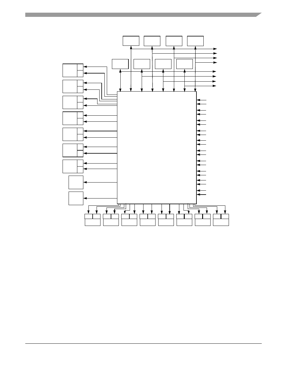
CPM Multiplexing
MPC8260 PowerQUICC II Family Reference Manual, Rev. 2
Freescale Semiconductor
16-5
Figure 16-3. Bank of Clocks
The eight BRGs also make their clocks available to external logic, regardless of whether the BRGs are
being used by a serial device. Notice that the BRG outputs are multiplexed with other functions; thus, all
BRGOx pins may not always be available.
Chapter 40, “Parallel I/O Ports,”
shows the function
multiplexing.
There are two restrictions in the bank-of-clocks mapping:
•
Only four of the twenty sources can be connected to any given FCC or SCC receiver or transmitter.
•
The SMC transmitter and receiver share the same clock source when connected to the NMSI.
shows the clock source options for the serial controllers and TDM channels.
BRG1
BRG2
BRG3
BRG4
CLK1
CLK2
BRGO1
BRGO2
BRGO3
BRGO4
Bank of Clocks
Selection Logic
CLK3
CLK4
CLK5
CLK6
CLK7
CLK8
CLK9
CLK10
CLK11
CLK12
CLK13
CLK14
CLK15
CLK16
BRG5
BRG6
BRG7
BRG8
BRGO5
BRGO6
BRGO7
BRGO8
FCC1
Tx
CLK17
CLK18
CLK19
CLK20
(Partially filled cross-switch logic
programmed in the CMX registers.)
Rx
FCC2
Tx
Rx
FCC3
Tx
Rx
SCC1
Tx
Rx
SCC2
Tx
Rx
SCC3
Tx
Rx
SCC4
Tx
Rx
SMC1
SMC2
TDMA1
Tx
Rx
TDMB1
Tx
Rx
TDMC1
Tx
Rx
TDMD1
Tx
Rx
TDMA2
Tx
Rx
TDMB2
Tx
Rx
TDMC2
Tx
Rx
TDMD2
Tx
Rx