Figure 13-5. output control cell (io.ctl), 4 instruction register, Instruction register -5 – Freescale Semiconductor MPC8260 User Manual
Page 537: Output control cell (io.ctl) -5, General arrangement of bidirectional pin cells -5, Figure 13-5, Figure 13-6
IEEE 1149.1 Test Access Port
MPC8260 PowerQUICC II Family Reference Manual, Rev. 2
Freescale Semiconductor
13-5
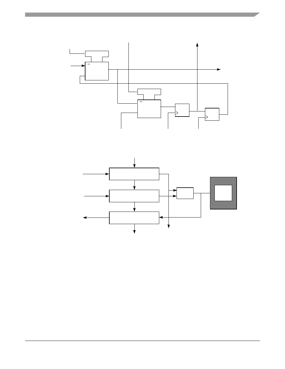
Figure 13-5. Output Control Cell (IO.CTL)
Figure 13-6. General Arrangement of Bidirectional Pin Cells
The control bit value controls the output function of the bidirectional pin. One or more bidirectional data
cells can be serially connected to a control cell. Bidirectional pins include two scan cell for data (IO.Cell)
as shown in
and these bits are controlled by the cell shown in
.
13.4
Instruction Register
The PowerQUICC II JTAG implementation includes the public instructions (EXTEST,
SAMPLE/PRELOAD, and BYPASS) and also supports the CLAMP instruction. One additional public
instruction (HI-Z) can be used to disable all device output drivers. The PowerQUICC II includes an 8-bit
instruction register (no parity) that consists of a shift register with four parallel outputs. Data is transferred
1
1
MUX
G1
1
1
MUX
G1
C
D
C
D
From Last Cell
Clock DR
Update DR
Shift DR
1 — EXTEST | Clamp
To Output
Buffer
0 — Otherwise
To Next Cell
Output Control
Logic
from System
I/O
Pin
From Last Cell
Output Data
Input Data
Output Enable
I.OBS
EN
from System Logic
O.PIN
I/O.CTL
To Next Pin Pair
To Next Cell