1 dma channel mode (dcm), Figure 19-9. dcm parameters, Dma channel mode (dcm) -19 – Freescale Semiconductor MPC8260 User Manual
Page 663: Dcm parameters -19, Section 19.8.2.1, “dma channel mode (dcm), Section 19.8.2.1, Dma channel mode (dcm)
SDMA Channels and IDMA Emulation
MPC8260 PowerQUICC II Family Reference Manual, Rev. 2
Freescale Semiconductor
19-19
19.8.2.1
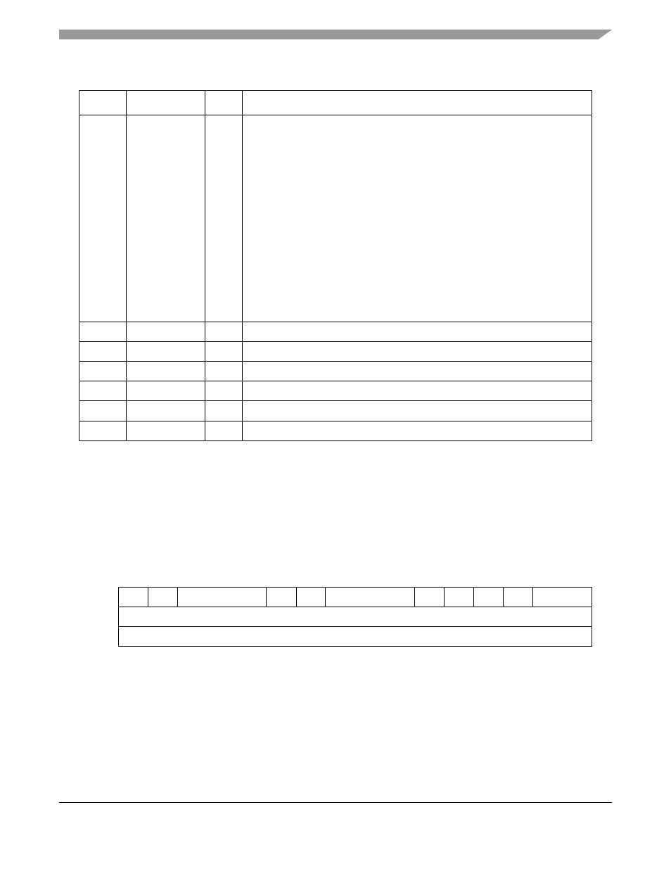
DMA Channel Mode (DCM)
The IDMA channel mode (DCM), shown in
, is a 16-bit field within the IDMA parameter
RAM, that controls the operation modes of the IDMA channel. As are all other IDMA parameters, the
DCM is undefined at reset.
describes DCM bits.
0x16
DTS
Hword Destination transfer size in bytes. All transfers to destination (except the start
alignment and the tail) are written to the bus using this parameter.
In peripheral-to-memory mode, DTS should equal SS_MAX.
In memory-to-peripheral modes, initialize DTS to the peripheral port size if
transfer’s destination is a peripheral. Valid sizes for peripheral destination is 1,
2, 4, and 8 bytes, or peripheral transfer size (if the peripheral accepts bursts).
See Table 19-8. for valid STS values for peripherals.
In fly-by mode, DTS is initialized to the peripheral port size.
• In memory-to-memory mode:
• DTS value is initialized to SS_MAX.
• STS value is initialized to SS_MAX. DTS can be initialized to values other
than SS_MAX in the following conditions:
– DTS must divide SS_MAX.
– DTS must be divided by 32, to enable bursts in steady-state phase.
• See Table 19-8. for valid memory-to-memory DTS values.
0x18
RET_ADD
Hword Used to save return address when working in ERM = 1 mode.
0x1A
—
Hword Reserved, should be cleared.
0x1C
BD_CNT
Word
Internal byte count.
0x20
S_PTR
Word
Source internal data pointer.
0x24
D_PTR
Word
Destination internal data pointer.
0x28
ISTATE
Word
Internal. Should be cleared before every
START
_
IDMA
command.
1
From the pointer value programmed in IDMA
x
_BASE: IDMA1_BASE at 0x87FE, IDMA2_BASE at 0x88FE,
IDMA3_BASE at 0x89FE, and IDMA4_BASE at 0x8AFE; see
Section 14.5.2, “Parameter RAM
0
1
2
4
5
6
7
9
10
11
12
13
14
15
Field
FB
LP
—
TC2
—
DMA_WRAP
SINC DINC ERM
DT
S/D
Reset
—
R/W
R/W
Figure 19-9. DCM Parameters
Table 19-4. IDMA
x Parameter RAM (continued)
Offset
1
Name
Width
Description