Table 40-6 shows the port b pin assignments – Freescale Semiconductor MPC8260 User Manual
Page 1289
Parallel I/O Ports
MPC8260 PowerQUICC II Family Reference Manual, Rev. 2
Freescale Semiconductor
40-11
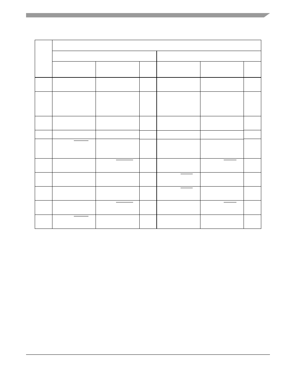
shows the port B pin assignments.
PA9
SMC2: SMTXD
TDM_A1: L1TXD[0]
Output, nibble
TDM_A1: L1TXD
Inout, serial
GND
PA8
SMC2: SMRXD
(primary option)
by PD4
TDM_A1: L1RXD[0]
Input, nibble
TDM_A1: L1RXD
Inout, serial
GND
PA7
SMC2: SMSYN
(primary option)
by PC0
TDM_A1:
L1TSYNC/GRANT
GND
PA6
TDM_A1: L1RSYNC
GND
PA5
SCC2: RSTRT
FCC1: RxPrty
1,3
UTOPIA
(secondary option)
GND
FCC2: RxAddr[2]
1
MPHY master
IDMA4: DREQ
GND
PA4
FCC2: RxAddr[1]
1
MPHY master
SCC2: REJECT
VDD
IDMA4: DONE
Inout
VDD
PA3
FCC2: RxAddr[0]
1
MPHY master
CLK19
GND
IDMA4: DACK
TDM_A2: L1RXD[1]
Nibble
GND
PA2
FCC2: TxAddr[0]
1
MPHY master
CLK20
GND
IDMA3: DACK
PA1
FCC2: TxAddr[1]
1
MPHY master
SCC1: REJECT
VDD
IDMA3: DONE
Inout
VDD
PA0
SCC1: RSTRT
FCC2: TxAddr[2]
1
MPHY master
IDMA3: DREQ
GND
1
Not available on the MPC8250.
2
MSNUM[0–4] is the sub-block code of the peripheral controller using SDMA; MSNUM[5] indicates which section,
transmit or receive, is active during the transfer. See
Section 19.2.4, “SDMA Transfer Error MSNUM Registers
3
.25
µm (HiP4) devices only: available only when the primary option for this function is not used.
Table 40-5. Port A—Dedicated Pin Assignment (PPARA = 1) (continued)
Pin
Pin Function
PSORA = 0
PSORA = 1
PDIRA = 1 (Output)
PDIRA = 0 (Input)
Defaul
t Input
PDIRA = 1 (Output)
PDIRA = 0 (Input, or
Inout if Specified)
Defaul
t Input