Figure 11-58, Figure 11-59 – Freescale Semiconductor MPC8260 User Manual
Page 486
Memory Controller
MPC8260 PowerQUICC II Family Reference Manual, Rev. 2
11-68
Freescale Semiconductor
NOTE
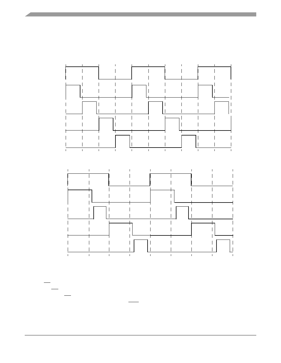
For integer clock ratios, the widths of T1/2/3/4 are equal, for a 1:2.5 clock
ratio, T1 = 4/3*T2 and T3 = 4/3*T4, and for a 1:3.5 clock ratio, the ticks
widths are T1 = 3/2*T2 and T3 = 3/2*T4.
Figure 11-58. Memory Controller UPM Clock Scheme for Integer Clock Ratios
Figure 11-59. Memory Controller UPM Clock Scheme for Non-Integer (2.5:1/3.5:1) Clock Ratios
The state of the external signals may change (if specified in the RAM array) at any positive edge of T1,
T2, T3, or T4 (there is a propagation delay specified in the Hardware Specifications). Note however that
only the CS signal corresponding to the currently accessed bank is manipulated by the UPM pattern when
it runs. The BS signal assertion and negation timing is also specified for each cycle in the RAM word;
which of the four BS signals are manipulated depends on the port size of the specified bank, the external
address accessed, and the value of TSIZn. The GPL lines toggle as programmed for any access that
initiates a particular pattern, but resolution of control is limited to T1 and T3.
CLKIN
T1
T2
T3
T4
CLKIN
T1
T2
T3
T4