Table 11-22. 60x address bus partition, 60x address bus partition -49 – Freescale Semiconductor MPC8260 User Manual
Page 467
Memory Controller
MPC8260 PowerQUICC II Family Reference Manual, Rev. 2
Freescale Semiconductor
11-49
11.4.12.1 SDRAM Configuration Example (Page-Based Interleaving)
Consider the following SDRAM organization:
•
64-bit port size, organized as eight 64-Mbit devices, each organized as 8M x 8bits.
•
Each device has 4 internal banks, 12 rows, and 9 columns
For page-based interleaving, the address bus should be partitioned as shown in
.
The following parameters can be extracted:
•
PSDMR[PBI] = 1—Page-based interleaving
•
ORx[BPD] = 01—Four internal banks
•
ORx[ROWST] = 0110—Row starts at A[6]
•
ORx[NUMR] = 011—Twelve row lines
Now, from the SDRAM device point of view, during an
ACTIVATE
command, its address port should look
like
Table 11-20 on page 11-38 indicates that to multiplex A[6–17] over A[17–28], PSDMR[SDAM] must be
011 and, because the internal bank selects are multiplexed over A[15–16], PSDMR[BSMA] must be 010
(only the lower two bank select lines are used).
When using bank-based interleaving, the internal bank-select signals that are multiplexed over the address
lines should be adjacent to the row address during the
ACTIVATE
command (refer to
). So, the
value of PSDMR[BSMA] is selected according to the combination of PSDMR[SDAM], ORx[ROWST],
and ORx[NUMR]. Otherwise, the output of the BNKSEL pins could be incorrect even if the device is
connected to the BNKSEL pins. To ensure proper connection, note that BNKSEL0 is msb and BNKSEL2
is lsb as stated in Table 6-1.
When using page-based interleaving, the internal bank-select signals that are mutilplexed over the address
lines are determined only by PSDMR[BSMA] during the
ACTIVATE
command. The output of the BNKSEL
pins are not affected by the PSDMR[BSMA] value.
During a
READ
/
WRITE
command, the address port should look like
.
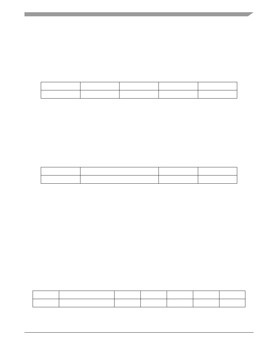
Table 11-22. 60x Address Bus Partition
A[0–5]
A[6–17]
A[18–19]
A[20–28]
A[29–31]
msb of start address
Row
Bank select
Column
lsb
Table 11-23. SDRAM Device Address Port during
ACTIVATE
Command
“A[0–14]”
A[15–16]
A[17–28]
A[29–31]
—
Internal bank select (A[18–19])
Row (A[6–17])
n.c.
Table 11-24. SDRAM Device Address Port during
READ
/
WRITE
Command
“A[0–14]”
A[15–16]
A[17]
A[18]
A[19]
A[20–28]
A[29–31]
—
Internal bank select
Don’t care
AP
Don’t care
Column
n.c.