Figure 13-1. test logic block diagram, Table 13-1. tap signals, 2 tap controller – Freescale Semiconductor MPC8260 User Manual
Page 534: Tap controller -2, Test logic block diagram -2, Tap signals -2, The tap consists of the signals in table 13-1
IEEE 1149.1 Test Access Port
MPC8260 PowerQUICC II Family Reference Manual, Rev. 2
13-2
Freescale Semiconductor
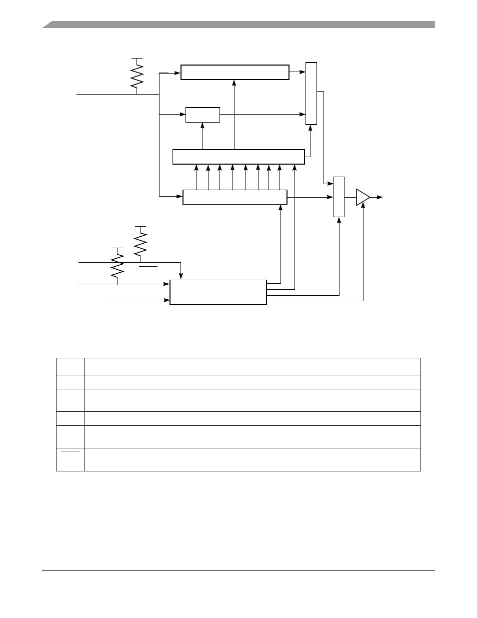
Figure 13-1. Test Logic Block Diagram
The TAP consists of the signals in Table 13-1.
.
13.2
TAP Controller
The TAP controller is responsible for interpreting the sequence of logical values on the TMS signal. It is
a synchronous state machine that controls the operation of the JTAG logic. The value shown adjacent to
each bubble represents the value of the TMS signal sampled on the rising edge of the TCK signal.
shows the state machine.
Table 13-1. TAP Signals
Signal Description
TCK
A test clock input to synchronize the test logic.
TMS
A test mode select input (with an internal pull-up resistor) that is sampled on the rising edge of TCK to
sequence the TAP controller’s state machine.
TDI
A test data input (with an internal pull-up resistor) that is sampled on the rising edge of TCK.
TDO
A data output that can be three-stated and actively driven in the shift-IR and shift-DR controller states. TDO
changes on the falling edge of TCK.
TRST
An asynchronous reset with an internal pull-up resistor that provides initialization of the TAP controller and
other logic required by the standard.
Boundary Scan Register
Bypass
M
U
X
Instruction Apply & Decode Register
8–Bit Instruction Register
M
U
X
TDO
TDI
TMS
TCK
TRST
TAP Controller
8
0