One-clock delay from sync to data (xfsd = 01) -20, No delay from sync to data (xfsd = 00) -20, Figure 15-12 – Freescale Semiconductor MPC8260 User Manual
Page 596: Figure 15-13
Serial Interface with Time-Slot Assigner
MPC8260 PowerQUICC II Family Reference Manual, Rev. 2
15-20
Freescale Semiconductor
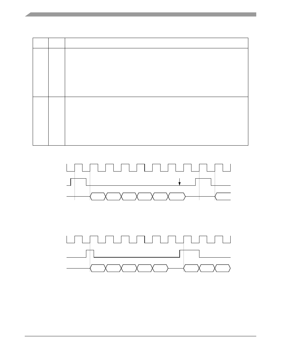
shows the one-clock delay from sync to data when xFSD = 01.
Figure 15-12. One-Clock Delay from Sync to Data (
xFSD = 01)
shows the elimination of the single-clock delay shown in
by clearing xFSD.
Figure 15-13. No Delay from Sync to Data (
xFSD = 00)
shows the effects of changing FE when CE = 1 with a 1-bit frame sync delay.
13
GMx
Grant mode for TDM a, b, c, or d
0 GCI/SCIT mode. The GCI/SCIT D channel grant mechanism for transmission is internally
supported. The grant is one bit from the receive channel. This bit is marked by programming the
channel select bits of the SI
x
RAM with 0111 to assert an internal strobe on it. See
Section 15.7.2.2, “SCIT Programming
.”
1 IDL mode. A grant mechanism is supported if the corresponding CMXSCR[GR
x
] bit is set. The
grant is a sample of L1GRx while L1RSYNCx is asserted. This grant mechanism implies the IDL
access controls for transmission on the D channel. See
Section 15.6.2, “IDL Interface
.”
14–15
TFSDx Transmit frame sync delay for TDM a, b, c or d. Determines the number of clock delays between the
transmit sync and the first bit of the transmit frame. See Figure 15-16..
00 No bit delay. The first bit of the frame is transmitted/received on the same clock as the sync. If
frame sync delay is not used and if a frame sync is issued early during the last bit of the
previous frame, data corruption could occur on all subsequent frames. To avoid this problem,
program a 1, 2, or 3-bit sync delay.
01 1-bit delay
10 2-bit delay
11 3-bit delay
Table 15-5. SI
xMR Field Descriptions (continued)
Bits
Name
Description
L1CLK
Data
(CE=0)
L1SYNC
(FE=1)
Bit-0
Bit-1
Bit-2
Bit-3
Bit-4
Bit-0
One-Clock Delay from Sync Latch to First Bit of Frame
Bit-5
End of Frame
L1CLK
Data
(CE=0)
L1SYNC
(FE=1)
Bit-0
Bit-1
Bit-2
Bit-3
Bit-4
No Delay from Sync Latch to First Bit of Frame
Bit-2
Bit-1
Bit-0