Table 30-49. ftirrx field descriptions, Figure 30-62. fcc transmit internal rate clocking, Fcc transmit internal rate registers (ftirrx) -92 – Freescale Semiconductor MPC8260 User Manual
Page 1012: Fcc transmit internal rate clocking -92, Ftirrx field descriptions -92
ATM Controller and AAL0, AAL1, and AAL5
MPC8260 PowerQUICC II Family Reference Manual, Rev. 2
30-92
Freescale Semiconductor
The first four PHY devices (address 00– 03) on FCC1 and FCC2 have their own transmit internal rate
registers (FTIRRx_PHY0–FTIRRx_PHY3) for use in transmit internal rate mode. In this mode, the total
transmission rate is determined by FCC internal rate timers. As a master, the controller only polls the
PHY’s Clav status at the rate determined by the internal rate. As a slave, the controller attempts to insert
cells into the FIFO at the internal rate. The controller can handle a lag of up to seven cells per PHY between
the programmable and actual bus rate. When the cell count mismatch reaches seven, TIRU event is
reported, see
Section 30.13.3, “ATM Event Register (FCCE)/Mask Register (FCCM).”
Note that a
mismatch occurs if the PHY rate or the CPM performance are lower then the internal rate. FTIRRx, shown
in
, includes the initial value of the internal rate timer. The source clock of the internal rate
timers is supplied by one of four baud-rate generators selected in CMXUAR; see
UTOPIA Address Register (CMXUAR).”
Note that in slave mode, FTIRRx_PHY0 is used regardless of
the slave PHY address.
describes FTIRRx fields.
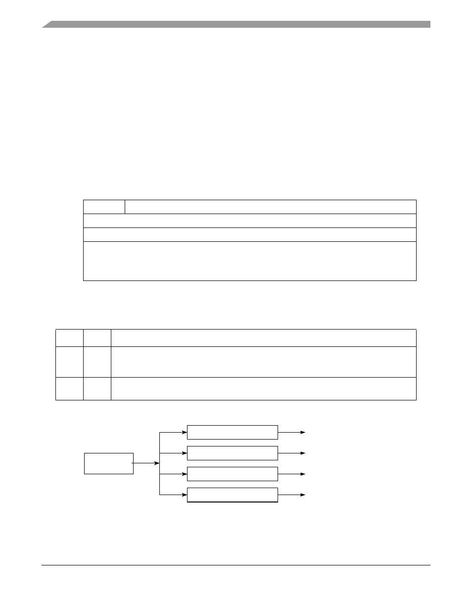
shows how transmit clocks are determined.
.
Figure 30-62. FCC Transmit Internal Rate Clocking
0
1
2
3
4
5
6
7
Field
TRM
Initial Value
Reset
0000_0000
R/W
R/W
Addr
FCC1: 0x0x1131C (FTIRR1_PHY0), 0x0x1131D (FTIRR1_PHY1),
0x0x1131E (FTIRR1_PHY2), 0x0x1131F (FTIRR1_PHY3)
FCC2: 0x0x1133C (FTIRR2_PHY0), 0x0x1133D (FTIRR2_PHY1),
0x0x11133E (FTIRR2_PHY2), 0x0x1133F (FTIRR2_PHY3)
Figure 30-61. FCC Transmit Internal Rate Registers (FTIRR
x)
Table 30-49. FTIRR
x Field Descriptions
Bits
Name
Description
0
TRM
Transmit mode.
0 External rate mode.
1 Internal rate mode.
1–7
Initial
Value
The initial value of the internal rate timer. A value of 0x7F produces the minimum clock rate (BRG
CLK divided by 128); 0x00 produces the maximum clock rate (BRG CLK divided by 1).
BRG CLK
PHY#0 Internal Rate Timer
PHY# 0 Tx Rate
PHY# 1 Tx Rate
PHY# 2 Tx Rate
PHY# 3 Tx Rate
PHY#3 Internal Rate Timer
PHY#2 Internal Rate Timer
PHY#1 Internal Rate Timer