Table 11-42. upms attributes example, Upms attributes example -82 – Freescale Semiconductor MPC8260 User Manual
Page 500
Memory Controller
MPC8260 PowerQUICC II Family Reference Manual, Rev. 2
11-82
Freescale Semiconductor
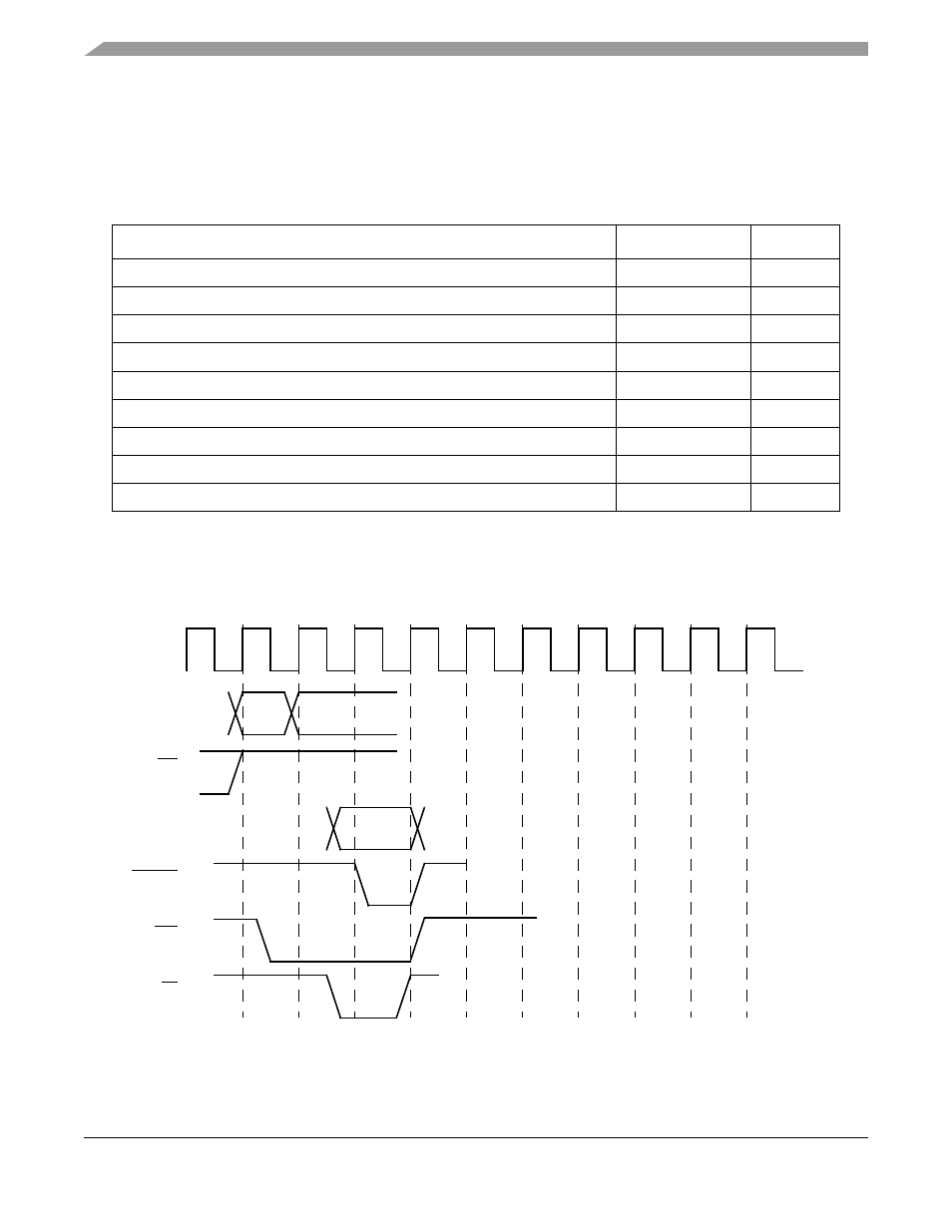
After timings are created, programming the UPM continues with translating these timings into tables
representing the RAM array contents for each possible cycle. When a table is completed, the global
parameters of the UPM must be defined for handling the disable timer (precharge) and the refresh timer
relative to
.
shows settings of different fields.
The OR and BR of the specific bank must be initialized according to the address mapping of the DRAM
device used. The MS field should indicate the specific UPM selected to handle the cycle. The RAM array
of the UPM can than be written through use of the MxMR[OP] = 11.
shows the first locations
addressed by the UPM, according to the different services required by the DRAM.
Table 11-42. UPMs Attributes Example
Explanation
Field
Value
Machine select UPMA
BR
x
[MS]
0b100
Port size 64-bit
BR
x
[PS]
0b00
No write protect (R/W)
BR
x
[WP]
0b0
Refresh timer value (1024 refresh cycles)
PURT[PURT]
0x0C
Refresh timer enable
M
x
MR[RFEN]
0b1
Address multiplex size
M
x
MR[AM
x
]
0b010
Disable timer period
M
x
MR[DS
x
]
0b01
Select between GPL4 and UPMWAIT = GPL4 data sample at clock rising edge
M
x
MR[GPL_x4DIS]
0b0
Burst inhibit device
OR
x
[BI]
0b0
CLKIN
A
RD/WR
D
PSDVAL
CS1
BS
Row
Column 1
(CAS)
(RAS)