1 signal configuration, Figure 7-1. signal groupings, 2 signal descriptions – Freescale Semiconductor MPC8260 User Manual
Page 258: Signal configuration -2, Signal descriptions -2, Signal groupings -2
60x Signals
MPC8260 PowerQUICC II Family Reference Manual, Rev. 2
7-2
Freescale Semiconductor
7.1
Signal Configuration
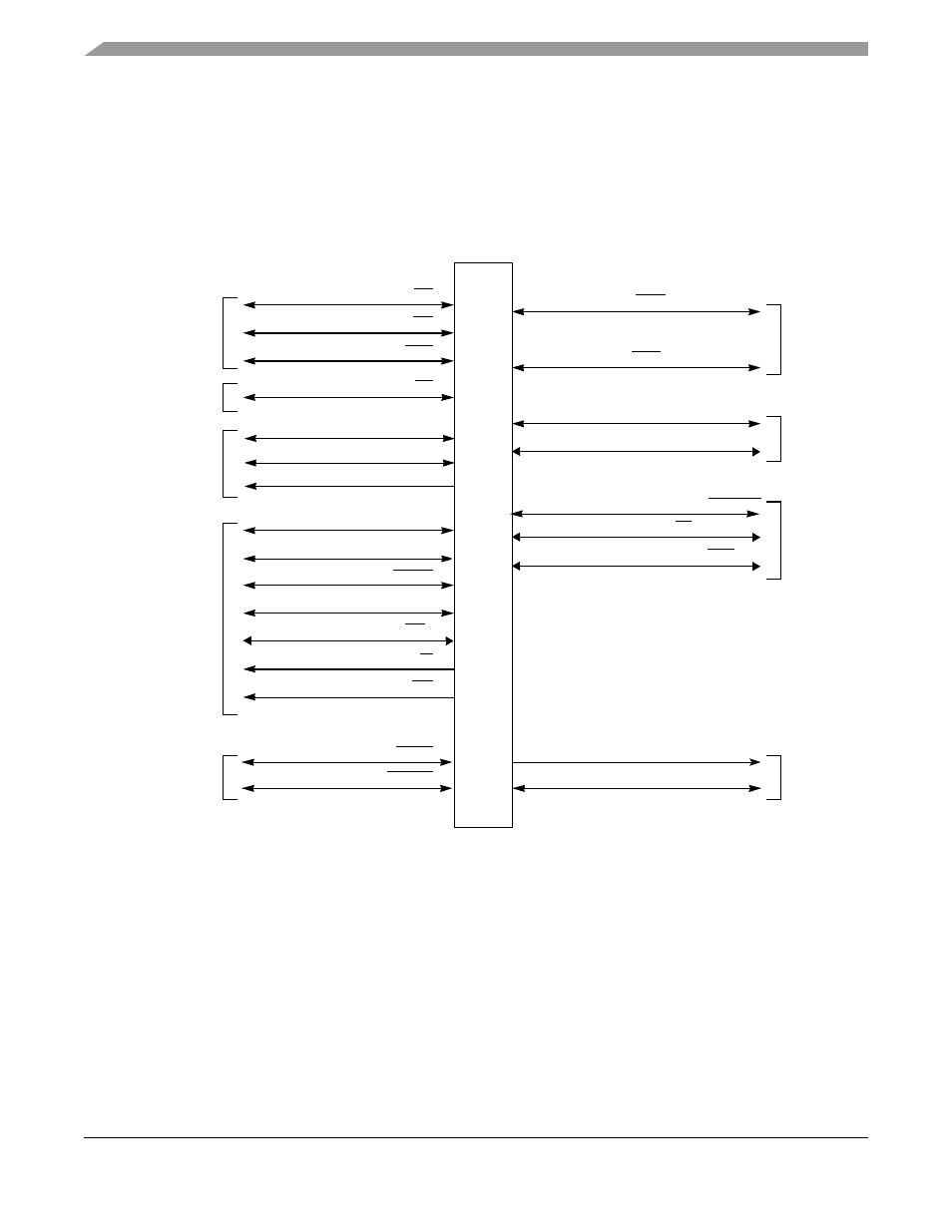
Figure shows the grouping of the PowerQUICC II’s 60x bus signal configuration.
NOTE
The PowerQUICC II hardware specifications provides a pinout showing pin
numbers. These are shown in
Figure 7-1. Signal Groupings
7.2
Signal Descriptions
This section describes individual PowerQUICC II 60x signals, grouped according to
. Note that
the following sections briefly summarize signal functions.
describes many of
these signals in greater detail, both in terms of their function and how groups of signals interact.
Bus Request (BR)
Bus Grant (BG)
Address Bus Busy (ABB)
Transfer Start (TS)
Address Parity (AP[0–3])
Transfer Size (TSIZ[0–3])
Transfer Burst (TBST)
Cache Inhibit (CI)
Write-Through (WT)
Address Acknowledge (AACK)
Address Retry (ARTRY)
Data Bus Grant (DBG)
Data Bus Busy (DBB)
Data (D[0–63])
Data Parity (DP[0–7])
Transfer Acknowledge (TA)
Transfer Error Acknowledge (TEA)
Reservation
1
1
1
1
1
64
8
1
1
1
4
5
4
1
1
1
1
1
Data
Data
Data
Processor
Address
Address
Address
Transfer
Attributes
Address
Termination
1
Transfer Type (TT[0–4])
Global (GBL)
1
TLBI SYNC
1
Partial Data Valid Indication (PSDVAL)
1
3
Transfer Code (TC[0–2])
Address (A[0–31])
32
Address Parity Error (APE)
1
State
Termination
Transfer
Arbitration
Arbitration
Start
Bus