3 spi command register (spcom), Figure 38-8. spcom-spi command register, Table 38-4. spcom field descriptions – Freescale Semiconductor MPC8260 User Manual
Page 1256: 5 spi parameter ram, Spi command register (spcom) -10, Spi parameter ram -10, Spcom—spi command register -10, Spcom field descriptions -10
Serial Peripheral Interface (SPI)
MPC8260 PowerQUICC II Family Reference Manual, Rev. 2
38-10
Freescale Semiconductor
38.4.3
SPI Command Register (SPCOM)
The SPI command register (SPCOM), shown in
, is used to start SPI operation.
describes the SPCOM fields.
38.5
SPI Parameter RAM
The SPI parameter RAM area is similar to the SCC general-purpose parameter RAM. The CP accesses the
SPI parameter table using a user-programmed pointer (SPI_BASE) located in the parameter RAM; see
Section 14.5.2, “Parameter RAM.”
The SPI parameter table can be placed at any 64-byte aligned address
in the dual-port RAM’s general-purpose area (banks 1–8, 11 and 12). Some parameter values must be
user-initialized before the SPI is enabled; the CP initializes the others. Once initialized, parameter RAM
values do not usually need to be accessed. They should be changed only when the SPI is inactive.
shows the memory map of the SPI parameter RAM.
6
TXB
Tx buffer. Set when the Tx data of the last character in the buffer is written to the Tx FIFO. Wait two
character times to be sure data is completely sent over the transmit signal.
7
RXB
Rx buffer. Set after the last character is written to the Rx buffer and the BD is closed.
0
1
7
Field
STR
—
Reset
0000_0000
R/W
Write Only
Addr
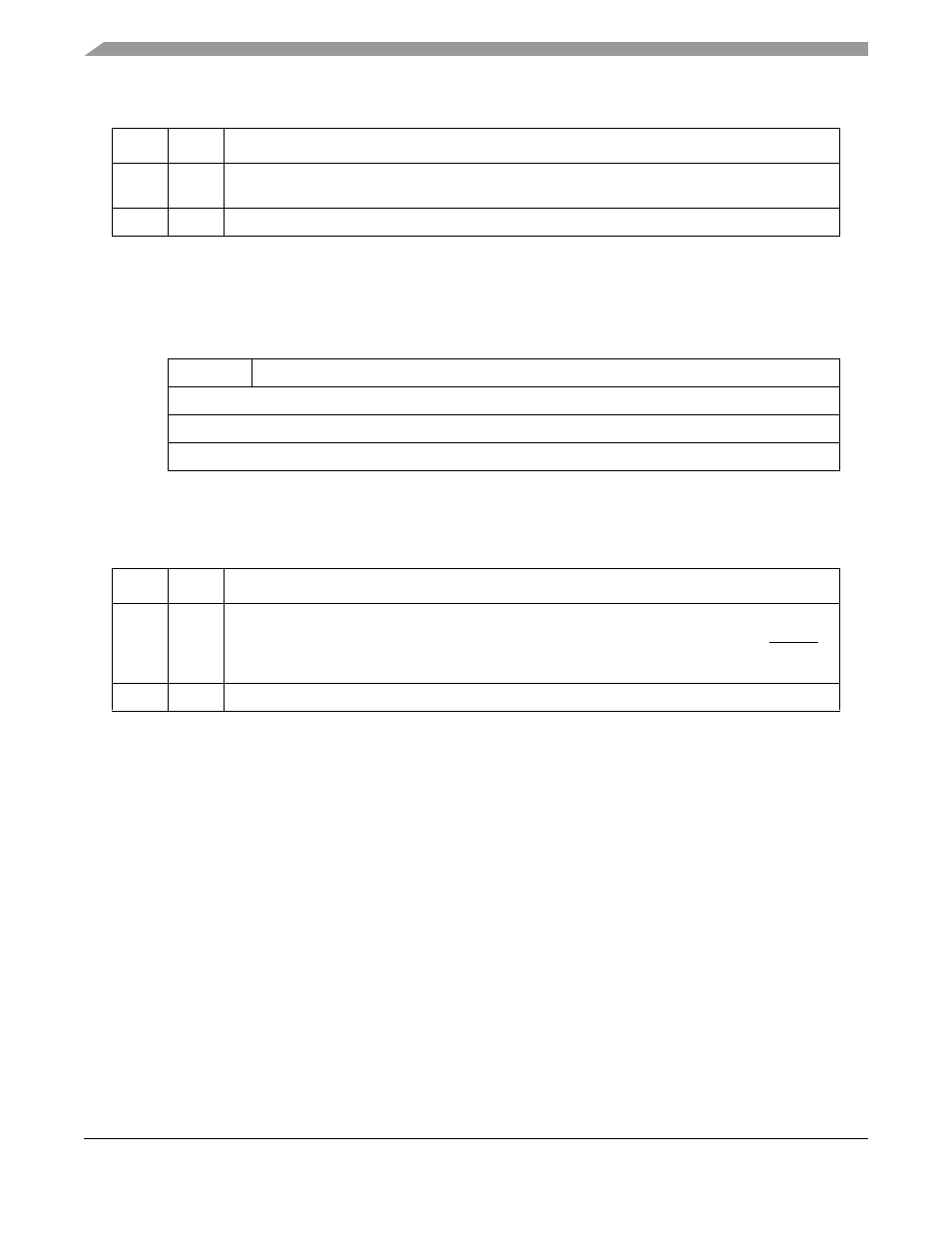
Figure 38-8. SPCOM—SPI Command Register
Table 38-4. SPCOM Field Descriptions
Bits
Name
Description
0
STR
Start transmit. For an SPI master, setting STR causes the SPI to start transferring data to and from
the Tx/Rx buffers if they are prepared. For a slave, setting STR when the SPI is idle causes it to load
the Tx data register from the SPI Tx buffer and start sending with the next SPICLK after SPISEL is
asserted. STR is cleared automatically after one system clock cycle.
1–7
—
Reserved and should be cleared.
Table 38-3. SPIE/SPIM Field Descriptions
Bits
Name
Description